
The reliable way to create a sine wave with a digital-to-analog converter (DAC) is to output digital samples from a sine lookup table at a precisely timed rate, then pass the DAC signal through a reconstruction low-pass filter. If the table has N samples and the DAC is updated at fs, repeating the table once per cycle produces fout = fs/N.
For example, a 256-entry table sent at 100,000 samples per second produces 390.625 Hz. A hardware timer and timer-triggered DMA normally provide more stable timing than a software delay loop.
How a DAC actually creates the sine wave
A DAC does not directly generate a mathematically continuous sine. It converts each digital code into a quantized voltage or current level. The result is usually a staircase or zero-order-held waveform: each value remains constant until the next update. Depending on the DAC architecture, the output may instead be a pulse-shaped or current signal requiring an external conversion stage.
The signal path is therefore:
sine samples → DAC codes → stepped analog output → reconstruction filter → loadA low-pass filter removes much of the energy around the sample frequency and its harmonics. TI explains the DAC reconstruction process in its overview of DAC output filtering: DAC reconstruction and analog filtering.
Free tools Windows power users keep installed
One-click scans. No signup required.
#1 Best Overall
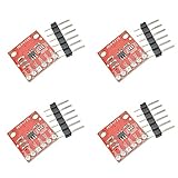
- The MCP4725 is a single-channel 12-bit buffered voltage output DAC with non-volatile memory (EEPROM) that allows you to store configuration register bits (2 bits) and DAC input data (12 bits) to non-volatile EEPROM (14-bit) In memory. The DAC can be configured for normal mode or power-saving shutdown mode by setting the configuration register bits.
- The DAC allows you to send analog signals, such as sine waves, from a digital source such as the I2C interface on an Arduino microcontroller. Digital to analog converters are ideal for sound generation, musical instruments and many other creative projects.
- This version of the CJMCU-MCP4725 Breakout solves some of the board's problems, including IC packages, I2C pinouts, changing the overall board size to better suit your project, and some minor adjustments.
- The board breaks down each pin you need to access and uses the MCP4725 (including GND and signal OUT pins) to connect to the oscilloscope or any other device you need to connect to the board. There are also SCL, SDA, VCC and another GND for the basic I2C pinout. The device can be used with a 2-wire I2C-compatible serial interface and is powered by a single supply from 2.7V to 5.5V.
- If you want more than one MCP4725 on the bus, you can disable the pull-up resistors on this board.
Choose the hardware before writing code
- A voltage-output DAC, or a current-output DAC with an appropriate voltage-conversion stage.
- A stable voltage reference and an analog output pin or connector.
- A hardware timer capable of the required sample rate.
- DMA support, preferably, or a timer interrupt for smaller designs.
- A reconstruction filter and, when necessary, an output buffer or amplifier.
- An oscilloscope or other instrument that can measure frequency, offset, amplitude and unwanted images.
Check the target device documentation for DAC resolution, code alignment, reference selection, trigger support, DMA request mapping, settling time, output-buffer limits and maximum update rate. An STM32-specific example is documented in ST’s DAC waveform-generation application note.
Build a sine lookup table
For an unsigned DAC, map the bipolar mathematical sine into the valid code range:
D[n] = Doffset + Dpeak sin(2πn/N)
Here, Doffset sets the center code and Dpeak sets the peak amplitude. For an M-bit DAC, the maximum code is 2M − 1. Midscale is approximately half that value.
This generic C code creates a 256-entry table for a 12-bit DAC. The clamp prevents an accidental configuration from writing an invalid code, but regular clamping indicates that the selected offset and amplitude are wrong.
#include <stdint.h>
#include <math.h>

#define TABLE_SIZE      256u
#define DAC_MAX         4095u
#define DC_OFFSET       2048u
#define PEAK_AMPLITUDE  1800u

static uint16_t sine_table[TABLE_SIZE];

static void build_sine_table(void)
{
    for (uint32_t i = 0; i < TABLE_SIZE; ++i) {
        float phase = 2.0f * 3.14159265358979323846f *
                      (float)i / (float)TABLE_SIZE;
        float value = (float)DC_OFFSET +
                      (float)PEAK_AMPLITUDE * sinf(phase);

        if (value < 0.0f) value = 0.0f;
        if (value > (float)DAC_MAX) value = (float)DAC_MAX;
        sine_table[i] = (uint16_t)(value + 0.5f);
    }
}
Precompute the table once for a fixed waveform instead of evaluating sinf() during every sample update. Microchip demonstrates this table-and-periodic-write method in its AVR DAC application note and its SAM waveform example.
Rank #2
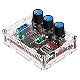
- Good Precision: the XR2206 function signal generator is precise, with a transparent case box shell for good assemble; Amplitude: 0-3V at 9V DC input; Distortion: less than 1% (at 1KHz); Flatness: +0.05dB 1Hz - 100kHz; Note:this set requires soldering tools; Please consult customer service for a detailed installation video
- Parameters: Voltage Supply: 9-12V DC Input; Waveforms: Square, Sine, Triangle; Impedance: 600 Ohm + 10%; Frequency: 1Hz-1MHz; Amplitude: 0-3V at 9V DC; InputDistortion: less than 1% (at 1KHz); Flatness: +0.05dB 1Hz - 100kaHz
- Sine wave parameters:Amplitude: 0-3V at 9V DC input; Distortion: less than 1% (at 1KHz); Flatness: +0.05dB 1Hz - 100kHz
- Square wave parameters: Amplitude: 8V (no load) at 9V DC Input; Rise Time: less than 50ns (at 1KHz); Fall Time: less than 30ns (at 1KHz); Symmetry: less than 5% (at 1KHz)
- Triangle wave: Amplitude: 0-3V at 9V DC input; Linearity: less than 1% (up to 100 KHz) 10 mA
Set the sample rate and output frequency
When a complete table is repeated once per cycle:
fout = fs / N
| DAC update rate | Table entries | Output frequency |
|---|---|---|
| 10 kS/s | 100 | 100 Hz |
| 48 kS/s | 256 | 187.5 Hz |
| 100 kS/s | 100 | 1 kHz |
| 1 MS/s | 256 | 3.90625 kHz |
A 12-bit DAC with a 3.3 V reference has an ideal code step of approximately 3.3/4095 = 0.806 mV. Its approximate output voltage is:
VOUT ≈ VREFD/(2M − 1)
For a 3.3 V system, midscale is about 1.65 V. A unipolar DAC cannot produce negative voltage; use a midpoint offset, an analog level-shifting stage, a bipolar-output DAC, or AC coupling if losing the DC component is acceptable.
Use a timer, interrupt or DMA for sample timing
A delay loop is useful for a demonstration but its timing changes with interrupt latency, floating-point work, compiler optimization, bus contention and operating-system scheduling. The preferred signal path is:
hardware timer → DAC trigger or DMA request → DAC data registerTimer interrupt
For a small, low-frequency project, an interrupt can write one table entry per timer event:
static volatile uint32_t index;

void sample_timer_callback(void)
{
    DAC_WRITE(sine_table[index]);
    index = (index + 1u) % TABLE_SIZE;
}
Keep the callback short. Do not perform variable-length calculations or blocking operations there.
Rank #3

- 12-bit resolutionI2C Interface (Standard, Fast, and High-Speed supported)Small package2.7V to 5.5V supplyInternal EEPROM to store settings
Timer-triggered DMA
DMA is the best general-purpose approach when the peripheral supports it. The timer generates a fixed-rate request, DMA reads the repeating table, and the DAC latches each value with minimal CPU involvement. TI’s DAC sine-DMA example uses a timer-triggered 20 kHz transfer.
- Build or place the sine table in accessible memory.
- Configure the DAC reference, channel and data alignment.
- Configure the timer for the desired sample rate.
- Configure circular DMA from the table to the DAC data register.
- Enable the DAC, DMA and timer in an order required by the target MCU.
- Measure the actual trigger rate and analog output rather than relying only on calculated settings.
Use DDS when the frequency must be tunable
A fixed table index produces frequencies tied to the sample rate and table length. Direct digital synthesis (DDS) keeps the sample clock fixed while changing frequency with a phase increment. On each sample, a phase accumulator wraps naturally and its upper bits select the sine-table entry:
Do these 3 things before closing this tab:
1Scan for outdated or missing drivers - takes under a minute2Clear out junk files and repair common Windows errors3Fix the driver behind crashes, sound loss and screen glitches#define PHASE_BITS 32u
#define TABLE_BITS 8u
static uint32_t phase_accumulator;
static uint32_t phase_increment;
void set_frequency(float output_hz, float sample_rate_hz)
{
phase_increment = (uint32_t)((output_hz / sample_rate_hz) *
4294967296.0f);
}
void dac_sample_callback(void)
{
phase_accumulator += phase_increment;
uint32_t index = phase_accumulator >> (PHASE_BITS - TABLE_BITS);
DAC_WRITE(sine_table[index]);
}For a 32-bit accumulator:
fout = fs × phase_increment / 232
At 100 kS/s and 1 kHz, the phase increment is approximately 42,949,673. DDS is useful for sweeps, modulation, multiple tones and FPGA designs. It can introduce phase-truncation spurs, amplitude quantization, interpolation error and finite-word frequency error. Analog Devices describes the phase accumulator and phase-to-amplitude conversion in its DDS overview and DDS HDL documentation.
Choose samples per cycle realistically
The theoretical Nyquist condition is fs > 2fout, but two or three samples per cycle rarely produce a useful analog sine. Tens of samples per cycle are a practical starting point for a simple generator; audio, measurement and low-distortion applications often need substantially more oversampling and filtering.
More table entries can reduce table-quantization effects, but they also increase memory and transfer traffic. If the sample rate stays fixed, increasing the table size lowers the maximum output frequency for a whole-cycle table. Quality also depends on DAC resolution, clock jitter, linearity, settling, filter response and measurement bandwidth.
Rank #4

- 【DDS Programmable Waveform Generation Core】 AD9833 uses direct digital synthesis technology; generates sine, triangle, and square waveforms; precise digital frequency control ensures stable output; supports signal generation tasks for learning, testing, and waveform evaluation in embedded systems
- 【Wide Frequency Control With High Resolution】 Supports finely adjustable output frequency based on DDS tuning words; clock‑dependent output up to 12.5 MHz; smooth frequency changes without mechanical tuning; enables accurate waveform setup for repeatable signal experiments
- 【SPI Digital Control Interface】 Configured through standard SPI communication using SCLK, SDATA, and FSYNC pins; simplifies integration with microcontrollers; enables fast register updates; improves reliability compared to analog tuning methods
- 【Wide 2.3 V To 5.5 V Power Compatibility】 Operates from 2.3 V to 5.5 V DC; supports both 3.3 V and 5 V logic systems; reduces external power constraints; improves flexibility when integrating into mixed‑voltage electronic projects
- 【Compact Module With Onboard Reference Clock】 Includes onboard crystal oscillator for stable timing reference; eliminates need for external clock sources; compact PCB layout simplifies wiring; compatible with for Arduino and similar SPI‑based controller platforms
Filter and buffer the DAC output
Use a reconstruction low-pass filter whose cutoff satisfies the first-pass relationship:
fout ≪ fc ≪ fs
A first-order RC filter has:
fc = 1/(2πRC)
For 1 kΩ and 10 nF, the cutoff is approximately 15.9 kHz. That may suit a 1 kHz signal at a much higher sample rate, but it is not a universal choice. Select the cutoff for acceptable amplitude droop and phase shift at the wanted frequency while attenuating sample-rate images. A higher-order active filter is preferable for audio or measurement work. Filtering cannot recover information lost through an inadequate sample rate, clipping or poor timing. See Analog Devices’ discussion of DDS bandwidth and output filtering.
Verify the output stage’s supply range, common-mode range, swing, slew rate, load current and stability with capacitive loads. A DAC pin may need a buffer before driving a cable or low-impedance load.
Independent reader supportYour contribution helps us test, update, and keep practical guides available for everyone.Hardware DAC versus PWM
A hardware DAC outputs multilevel codes directly. PWM instead varies duty cycle and relies on a filter:
PWM duty cycle → RC or active filter → approximate analog voltagePWM is useful when no DAC is available or the signal is slow and ripple is acceptable, but it leaves carrier energy, has different resolution limits and can create audible or electromagnetic interference. A board’s analogWrite() commonly controls PWM rather than a true DAC. TI documents a PWM sine-generation alternative in this application example; Microchip covers PWM and R-2R alternatives in AN655.
The Tool Desk
Outbyte PC Repair FREEClear out junk files and repair common Windows errorsFree Scan →Outbyte Driver Updater FREEFix the driver behind crashes, sound loss and screen glitchesFind Drivers →Best Value

- Combined with oscilloscope, it can be used for electronic circuit test and debugging, frequency characteristic and impulse response test and measurement of audio amplifier. Because DDS has good accuracy and frequency stability, it is also very suitable for oscilloscope scanning time factor calibration. The square wave output is suitable for oscilloscope attenuator and probe pulse characteristic adjustment. Has filters to accommodate the output of sine wave and pulse wave.
- DC4-9V power supply is recommended when using adapters, and 3.7V lithium batteries are recommended when using battery power. Current :180MA, voltage 5V, DC bias: maximum ±10V, with shutdown function. All Settings can be saved. There are filters that can be turned on and off, which can be well adapted to sinusoidal and pulse waveform output
- Frequency range: sine wave 0.01Hz-500.00 kHz(with the further increase of frequency, the output amplitude will decrease), other waveforms 0.01Hz-100.00 khz(but does not limit the upper limit of adjustable frequency, if the distortion and jitter requirements are not high, the use of frequency can be further increased).
- MODE: The mode key is used to change the output waveform. RUN/STOP: runs or stops the waveform output. When the cursor does not blink, output waveform. DCOFFSET: DC bias switch, adjust the DC component of the signal by pressing the yellow knob ON. Ejected to OFF, the DC component of the signal is 0. FILTER: Filter switch, when the signal is close to more than 300K sine wave, press this button, the waveform will be clean. AMP: Side keys adjust signal amplitude
- [Satisfactory Service]: We Provide 24-hour online service,If you encounter any problems, Please email SELLER SUPPORT (Not Amazon support), we will give you a perfect solution.
Architecture choices
| Approach | Use it when | Main trade-off |
|---|---|---|
| Lookup table plus timer interrupt | Learning, fixed low-frequency output, small MCU | CPU and interrupt jitter on every sample |
| Lookup table plus timer-triggered DMA | Most embedded waveform playback | Requires correct timer, DMA and DAC routing |
| DDS/NCO plus DAC | Fine tuning, sweeps, modulation or FPGA work | Spurs and quantization require careful design |
| PWM plus filter | Low cost and low-frequency signals | Carrier ripple and stronger filter dependence |
| Dedicated DDS IC | Standalone, agile waveform generation | Still needs clocking, filtering and suitable output conditioning |
| External precision DAC | Internal DAC lacks speed, resolution, linearity or channels | Additional interface, reference and analog hardware |
Troubleshoot by symptom
Wrong frequency
- Measure the actual timer or DMA trigger rate.
- Confirm table length, timer clock and prescaler.
- Check DMA circular mode, transfer width and request mapping.
- For DDS, verify the accumulator width used in the phase-increment calculation.
Clipping or flattened peaks
Offset plus amplitude may exceed the DAC range, the reference may be lower than expected, or an amplifier may lack output swing. Leave rail headroom and treat frequent code clamping as a design error.
Large visible steps
Possible causes include too few samples, low DAC resolution, no reconstruction filter or an output frequency too close to the sample rate. Increasing table size alone does not help if the update rate remains unchanged.
High-frequency images or PWM ripple
Use a lower filter cutoff, a higher-order filter or a higher sample/carrier rate. Measure both before and after filtering.
Glitches at code transitions
DAC glitch energy, asynchronous latching, bus timing and digital feedthrough can all contribute. Consult the DAC’s glitch and settling specifications and check grounding and layout.
What’s actually slowing this PC down?
Pick the symptom - the matching free tool is one click away.
Noise or unexpected offset
Check reference and supply noise, ground bounce, digital switching, probe technique, intentional midpoint offset, amplifier error and whether the instrument is AC- or DC-coupled. Measure average voltage and peak-to-peak voltage with DC coupling enabled.
Verify the finished waveform
- Measure frequency against the timer or DDS calculation.
- Measure DC offset and peak-to-peak amplitude at the actual load.
- Inspect the unfiltered DAC output and filtered output separately.
- Use FFT or spectrum measurement to check harmonics and sample-rate images.
- Test at minimum and maximum intended load and across the expected reference-voltage range.
- For demanding applications, account for DAC INL/DNL, glitch energy, settling time, clock jitter, reference noise and output-buffer limitations. Analog Devices discusses these nonidealities in its DDS sine-wave article.
The Bottom Line
For most projects, use a precomputed sine table, a hardware-timed sample clock and circular DMA into the DAC, followed by a filter selected for the desired frequency and sample rate. Add DDS when frequency must be changed precisely without changing the sample clock.
Quick Recap
Product prices and availability are accurate as of the date/time indicated and are subject to change. Any price and availability information displayed on Amazon at the time of purchase will apply.

