
Short answer: ASML’s February 2024 plan to ship “multiple” High-NA EUV systems in 2025 was a production expectation, not a disclosed shipment quota. The contemporaneous report said between 10 and 20 systems had been ordered by leading logic and memory manufacturers, while ASML was preparing capacity for approximately 20 systems per year by 2028. The exact number shipped in calendar 2025 has not been verified by a directly accessible primary-source tally.
The distinction matters because an order, a shipment, an installed scanner and a tool qualified for high-volume manufacturing are different milestones. High-NA was moving from first-customer process development toward early production, not replacing conventional EUV overnight.
What High-NA EUV changes
Extreme ultraviolet lithography uses 13.5-nanometer light to print some of the most demanding layers in advanced chips. Conventional EUV scanners, ASML’s NXE platform, use a numerical aperture (NA) of 0.33. The newer EXE platform raises NA to 0.55.
ASML lists approximately 8 nm optical resolution for High-NA, compared with approximately 13 nm for conventional EUV. That is an imaging specification, not an 8 nm process node: “2 nm” and similar labels describe entire process generations involving many layers, materials and design rules.
Quick wins for a faster PC:
Scan for outdated or missing drivers - takes under a minuteDriver Scan →Clear out junk files and repair common Windows errorsFree Scan →#1 Best Overall

- Precision Wafer Handling Tool: Designed for safe and precise handling of silicon wafers, semiconductor chips, and flat substrates during inspection, processing, evaporation, and laboratory applications.
- High-Purity PEEK Material Construction: Made from high-performance PEEK (Polyether Ether Ketone) polymer, offering excellent mechanical strength, low contamination characteristics, and suitability for semiconductor and precision laboratory environments.
- High Temperature & Chemical Resistance: PEEK material provides excellent thermal stability and supports short-term exposure up to approximately 300°C while maintaining strength and dimensional stability. Resistant to many chemicals and solvents.
- Flat Tip Wide Jaw Design: Features a flat tip and wide gripping jaw structure to provide stable and gentle handling of delicate wafers and flat samples while reducing surface contact impact.
- Low Outgassing & Long-Term Durability: Designed with low outgassing, low moisture absorption, wear resistance, and excellent dimensional stability, making it suitable for cleanroom, semiconductor fabrication, research, and inspection applications.
Higher NA can resolve smaller features and may reduce the number of times a difficult layer must be patterned. ASML says that reducing multiple-patterning steps could lower defects, cycle time and manufacturing cost. Those are potential system-level benefits, not guaranteed savings. Resist behavior, masks, overlay, inspection, etch, deposition, yield and throughput determine the result.
High-NA also does not eliminate other equipment. ASML expects NXE and EXE EUV systems to coexist, while DUV lithography and the rest of the process flow remain necessary for many layers. See ASML’s product explanation at ASML’s EUV lithography systems page.
The timeline from first delivery to planned production
- December 2023: ASML says it delivered the first High-NA EUV system. The initial purpose was process development and customer learning.
- January 2024: Intel announced receipt of the first EXE:5000 shipment at its Oregon site, according to contemporaneous reporting.
- February 14, 2024: AnandTech reported that ASML expected to ship multiple High-NA tools during 2025 and was preparing for approximately 20 systems of annual capacity by 2028.
- 2025–2026: ASML’s product documentation identified this period as the expected beginning of High-NA support for high-volume manufacturing, initially for advanced logic and later for memory.
The original report is available from AnandTech; an accessible archived copy is at this archive.
Rank #2

- for ultimate for surface Protection: Crafted from for premium PEEK material, these flat-tip tweezers for ensure scratch-free handling of sensitive wafers and semiconductors by point-loading damage during critical assembly tasks.
- Advanced for esd Safety: Designed with inherent anti-static properties to safely dissipate electrostatic charges, protecting delicate microelectronics and fiber optic components from discharge damage in cleanroom environments.
- Extreme Durability & Resistance: Withstands temperatures from -200°C to +260°C and resists harsh acids and alkalis used in etching, making these non-magnetic tools for ideal for diverse industrial and lab applications.
- for versatile Precision Toolset: Perfect for electronics repair, jewelry making, model building, and device assembly; the ergonomic design offers superior grip for long-term use in detailed soldering or inspection work.
- Reliable Quality Assurance: We stand behind our precision instruments with dedicated customer support; contact us immediately for any issues regarding product performance or satisfaction for a hassle-free resolution.
How many tools were involved?
| Figure | What it means | Qualification |
|---|---|---|
| “Multiple” in 2025 | A directional shipment expectation | The February 2024 report did not disclose an exact number. |
| 10–20 systems | Reported High-NA orders across leading logic and memory makers | An order range, not a confirmed 2025 shipment total. |
| Approximately 20 per year by 2028 | Reported annual production-capacity target | A preparation goal, not proof that 20 tools shipped or entered production. |
Orders can represent a purchase commitment, a reserved delivery slot or a future system awaiting site readiness. A shipped tool may still require installation, calibration, process qualification and yield learning. As of the evidence available for this article, no directly accessible primary source establishes the exact number of High-NA scanners shipped during calendar 2025.
What’s actually slowing this PC down?
Pick the symptom - the matching free tool is one click away.
Which chipmakers were associated with the orders?
The contemporaneous report said ASML had announced orders from major logic and memory manufacturers, including:
- Intel
- Samsung Foundry
- TSMC
- Micron
- Samsung’s memory operation
- SK hynix
It did not publish a customer-by-customer allocation, contract date or delivery schedule. Therefore, the report supports saying these companies were associated with announced orders; it does not support assigning each company a number of tools or claiming that all had already qualified High-NA for volume production.
Rank #3

- Precision Wafer Handling Tool: Designed for safe and precise handling of silicon wafers, semiconductor chips, and flat substrates during inspection, processing, evaporation, and laboratory applications.
- High-Purity PEEK Material Construction: Made from high-performance PEEK (Polyether Ether Ketone) polymer, offering excellent mechanical strength, low contamination characteristics, and suitability for semiconductor and precision laboratory environments.
- High Temperature & Chemical Resistance: PEEK material provides excellent thermal stability and supports short-term exposure up to approximately 300°C while maintaining strength and dimensional stability. Resistant to many chemicals and solvents.
- Flat Tip Wide Jaw Design: Features a flat tip and wide gripping jaw structure to provide stable and gentle handling of delicate wafers and flat samples while reducing surface contact impact.
- Low Outgassing & Long-Term Durability: Designed with low outgassing, low moisture absorption, wear resistance, and excellent dimensional stability, making it suitable for cleanroom, semiconductor fabrication, research, and inspection applications.
Why ASML needed more production capacity
A High-NA ramp is broader than adding assembly space at ASML. Capacity must expand across a tightly coordinated chain:
- large, high-precision projection optics and other optical modules;
- light-source, mechatronic and wafer-stage subsystems;
- final assembly, testing and customer acceptance;
- clean-room floor space, power, cooling and vibration control at customer fabs;
- installation, field service and specialist engineering personnel;
- reticle, resist, metrology, inspection, etch and deposition infrastructure needed to make the scanner useful.
The reported 2028 target therefore describes an ecosystem and delivery capability, not simply a promise to build more identical machines in one factory.
Do these 3 things before closing this tab:
1Fix the driver behind crashes, sound loss and screen glitches2Repair Windows errors before they cause bigger problems3Scan for outdated or missing drivers - takes under a minuteThe economic question: can a roughly €350 million scanner pay back?
The archived 2024 report put an indicative High-NA Twinscan EXE price at about €350 million (approximately $380 million at the time). It cited about €170 million (approximately $183 million) for a conventional NXE EUV system. These were reported 2024 estimates, not current official list prices; ASML does not generally publish a public price list for individual customer systems.
Rank #4
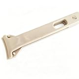
- Precision Wafer Handling Tool: Designed for safe and precise handling of silicon wafers, semiconductor chips, and flat substrates during inspection, processing, evaporation, and laboratory applications.
- High-Purity PEEK Material Construction: Made from high-performance PEEK (Polyether Ether Ketone) polymer, offering excellent mechanical strength, low contamination characteristics, and suitability for semiconductor and precision laboratory environments.
- High Temperature & Chemical Resistance: PEEK material provides excellent thermal stability and supports short-term exposure up to approximately 300°C while maintaining strength and dimensional stability. Resistant to many chemicals and solvents.
- Flat Tip Wide Jaw Design: Features a flat tip and wide gripping jaw structure to provide stable and gentle handling of delicate wafers and flat samples while reducing surface contact impact.
- Low Outgassing & Long-Term Durability: Designed with low outgassing, low moisture absorption, wear resistance, and excellent dimensional stability, making it suitable for cleanroom, semiconductor fabrication, research, and inspection applications.
The relevant comparison is not simply one scanner against another. A chipmaker must compare High-NA capital cost with the cost of achieving the same pattern using lower-NA EUV, potentially including:
- additional exposures and masks;
- extra process, etch and deposition steps;
- longer cycle time and more constrained fab capacity;
- additional defect opportunities and yield loss;
- engineering and process-development expense.
High-NA becomes attractive when those avoided costs, plus adequate throughput and yield, offset the scanner’s depreciation and operating burden. It can be delayed when conventional EUV remains adequate, production volume is too low to amortize the tool, or the surrounding process ecosystem is not ready.
Independent reader supportYour contribution helps us test, update, and keep practical guides available for everyone.Why deployment could be slower than the headline suggested
Installation is a fab project
The optics and mechanical systems are substantially more demanding than those in existing EUV scanners. Sites need prepared foundations, vibration control, power, cooling, logistics routes and clean-room capacity before installation can begin.
Recommended Free Tools
Best Value
- for ultimate for surface Protection: Crafted from for premium PEEK material, these flat-tip tweezers for ensure scratch-free handling of sensitive wafers and semiconductors by point-loading damage during critical assembly tasks.
- Advanced for esd Safety: Designed with inherent anti-static properties to safely dissipate electrostatic charges, protecting delicate microelectronics and fiber optic components from discharge damage in cleanroom environments.
- Extreme Durability & Resistance: Withstands temperatures from -200°C to +260°C and resists harsh acids and alkalis used in etching, making these non-magnetic tools for ideal for diverse industrial and lab applications.
- for versatile Precision Toolset: Perfect for electronics repair, jewelry making, model building, and device assembly; the ergonomic design offers superior grip for long-term use in detailed soldering or inspection work.
- Reliable Quality Assurance: We stand behind our precision instruments with dedicated customer support; contact us immediately for any issues regarding product performance or satisfaction for a hassle-free resolution.
Resolution is not production economics
A nominal optical resolution does not establish wafer throughput, stochastic-defect performance, overlay or yield. Customers must tune resist, masks, computational lithography, inspection and downstream process steps as one flow.
Early systems are learning platforms
ASML described the first delivery as a process-development milestone, with high-volume-manufacturing support expected in the 2025–2026 window. A development tool can be commercially important without producing saleable high-volume wafers immediately.
Conventional EUV remains a moving target
Chipmakers can continue extending 0.33-NA EUV through process optimization and multiple patterning. High-NA adoption depends on when that alternative becomes more expensive or capacity-constrained than buying and integrating an EXE system.
What adoption forecasts actually said in 2024
The February 2024 coverage reported differing expectations. Intel was expected to introduce High-NA in a post-18A process around 2026–2027. Some analysts placed broader economic adoption around 2030–2031, while ASML executives argued that process simplification could justify earlier deployment around 2026–2027. These were forecasts made at the time, not verified outcomes, and they should not be read as identical schedules for Intel, TSMC, Samsung, Micron or SK hynix.
What ASML’s 2025 financial results do—and do not—show
ASML reported 2025 full-year net sales of €32.7 billion, a 52.8% gross margin, €4.7 billion in research and development costs and basic earnings per share of €24.73. Those company-wide figures, reported at ASML’s Q4 2025 results page, show the scale of the supplier but do not disclose High-NA shipment volume, installation status, customer acceptance, throughput or yield.
Quick Recap
What the 2025 shipment headline did—and did not—prove
- It referred to a genuine February 2024 report about an early commercial-production ramp.
- “Multiple tools” was not an exact 2025 shipment commitment.
- The reported 10–20 figure was an order range, not a shipment count.
- Approximately 20 systems per year by 2028 was a reported capacity target.
- High-NA’s strategic value depends on total manufacturing economics, not resolution alone.
Product prices and availability are accurate as of the date/time indicated and are subject to change. Any price and availability information displayed on Amazon at the time of purchase will apply.

