
The Tool Desk
Outbyte Driver Updater FREEFix the driver behind crashes, sound loss and screen glitchesFind Drivers →Outbyte PC Repair FREEClear out junk files and repair common Windows errorsFree Scan →To keep a buck or boost converter efficient as switching frequency rises, control the losses paid on every cycle: MOSFET switching and gate-drive loss, dead-time loss, magnetic AC and core loss, and parasitic loss from layout. Choose the lowest frequency that meets ripple, size, transient-response, and EMI requirements; then verify the complete design across its operating range. There is no universal “best” high frequency: the useful operating point is where the smaller passives or faster response still justify the added loss and thermal stress.
What changes when switching frequency rises?
Higher frequency means the converter completes more switching cycles per second. That can reduce the inductance and capacitance needed for a given ripple target and can support greater control bandwidth, but it also repeats switching transitions more often. Analog Devices notes that switching loss can dominate conduction loss at high frequencies because it scales with frequency.
The result is a design trade-off, not a one-way efficiency improvement. Smaller inductors and capacitors may reduce board area, but higher loss can require more thermal capacity, copper, or EMI filtering. Faster control response may help transient performance, while edge rate and parasitic ringing can make EMI and device stress harder to manage. Component availability and cost also matter: a theoretically suitable high-frequency part is not useful if its losses, thermal limits, or supply situation make the design impractical.
A measured frequency change is application-specific
ROHM’s 2019 calculated example for a 10 W, 5 V, 2 A supply shows how strongly the result can depend on the design. The figures below belong to that example; they are not a prediction for other converters.
What’s actually slowing this PC down?
Pick the symptom - the matching free tool is one click away.
#1 Best Overall

- Features: Built with SANYO solid capacitors, 36μ thick PCB, high-Q inductors, and an LED output indicator for enhanced performance and reliability.
- Application: Perfect for DIY power bank projects, powering monitors, communication devices, and a wide range of other electronic equipment.
- Wide Input Voltage Range: The LM2596 buck converter supports a broad input voltage range from 3V to 40V, making it ideal for various applications, including DIY electronics, solar power systems, and more.(Input voltage must be at least 1.5V higher than the output voltage; no boost function)
- High-Efficiency Output: Achieve up to 92% conversion efficiency with this step-down regulator, ensuring stable and efficient voltage regulation for your devices, from 1.25V to 35V.
- Adjustable Voltage Regulator: Easily customize the output voltage with a precision multi-turn potentiometer, providing flexibility for powering a wide range of electronic projects and devices.
| Switching frequency | Calculated loss | Calculated efficiency |
|---|---|---|
| 0.1 MHz | 0.632 W | 94.1% |
| 1 MHz | 1.208 W | Approximately 89.2% |
| 2 MHz | 1.848 W | 84.4% |
In this calculation, moving from 1 MHz to 2 MHz reduced efficiency by as much as 4.8 percentage points. Conversely, Analog Devices AN-140 reports a different example: a 12 V input, 3.3 V output synchronous buck rated for 10 A had about 2% to 5% efficiency loss from AC-related losses at 200–500 kHz, with about 93% overall efficiency at full load. Neither result sets a universal frequency limit; topology, parts, operating conditions, and loss accounting differ.
Build a loss budget before changing parts
Estimate each material loss term rather than relying on a single headline efficiency figure. Switching loss generally rises with frequency because transition energy is paid more often; conduction loss depends on current and the resistance or forward drop in the current path. At high frequency, the balance can shift enough that a low-resistance switch is no longer the best choice if its capacitance makes transitions expensive.
- MOSFET conduction: estimate loss from the device’s on-resistance at the actual gate voltage and operating temperature, together with its current waveform.
- Turn-on and turn-off: account for voltage-current overlap during transitions and the influence of gate charge and device capacitance. Include reverse-recovery effects where relevant.
- Gate drive: estimate approximately as VDRV × QG × fS, using the driver voltage, gate charge, and switching frequency. Gate-drive demand therefore grows with both gate charge and frequency.
- Dead time and body diode: include the interval when current flows through a body diode or other diode path, plus the timing and recovery effects of the chosen rectification scheme.
- Inductor: include winding DCR loss, frequency-dependent winding AC loss, and core loss. Core loss includes hysteresis and eddy-current contributions.
- Capacitors and PCB: include capacitor ESR heating from ripple current, relevant ESL effects, and PCB copper loss. Check capacitance reduction under DC bias where applicable.
- Other terms: include controller quiescent current, snubber or clamp dissipation, and any other intentional or parasitic loss in the power path.
Revisit the estimates at minimum and maximum input voltage, across the load range, at relevant temperatures, and at each candidate frequency. A design that looks efficient at full load may behave differently at light load or at a line-voltage extreme.
Choose the frequency from the design constraints
Begin at the lowest frequency that meets the converter’s ripple, transient-response, magnetics-size, and EMI requirements. Raise it only while the modeled or measured loss remains acceptable and the benefit is meaningful. Higher frequency can shrink filter components and support greater bandwidth, but it also raises switching and thermal losses.
Rank #2

- Mini MP1584EN DC to DC buck converter module with a wide operating range
- Input voltage: 4.5 V to 28 V; Output voltage: 0.8 V to 20 V
- Output current: 3 A (maximum); Conversion efficiency: 92% (maximum)
- Output ripple: less than 30 mV; Switching frequency: 1.5 MHz (highest), typically 1 MHz
- Operating temperature: -45 ℃ to 85 ℃; Size: 22 mm by 17 mm by 4 mm; Warning: do not reverse the positive and negative terminals to avoid any possible damage; Do not use light load (less than 10% of output power) or without load
Analog Devices AN-140 describes many step-down supplies at or above 10 A operating from 100 kHz to 1–2 MHz, while lower-current designs may reach several megahertz. Those are reported ranges, not recommended settings for every design. The suitable point depends on the specific size, cost, efficiency, and operating constraints.
Compare candidate settings across the whole system, not just inductor size. Account for the possibility that a smaller magnetic component will be offset by a larger heatsink, more PCB copper, or extra EMI filtering. Consider whether the improved transient response is needed for the actual load profile, and whether the design can maintain acceptable efficiency and temperature at light and full load.
Select switches and rectification for the chosen frequency
Balance MOSFET resistance against switching charge
A low RDS(on) reduces conduction loss, but achieving it with a larger die can bring higher capacitance and gate charge, increasing transition and drive losses. Compare RDS(on), QG, QGD, and relevant output and reverse-transfer capacitances at the intended operating conditions. Favor a device with suitably low resistance and manageable switching charge for the selected frequency; the lowest resistance alone is not a complete selection rule.
Use a gate voltage within the MOSFET rating and evaluate the resulting resistance benefit against the added gate-drive power. Gate resistance and drive strength affect edge timing, ringing, and switching loss, so verify their effects in the actual layout rather than assuming the fastest edge is best.
Rank #3

- 【Ultra-Compact】 Miniature size (17.5x12.3x4.3mm) with 5V stable output, ideal for ESP32 and Arduino and other projects.
- 【1.8A High-Current Output with Low Ripple】Delivers up to 1.8A continuous current (4.6V/1.5A) ensuring clean power for sensitive ICs. High-frequency switching (1.5MHz max) minimizes noise.
- 【Built for Demanding Applications】Robust heat dissipation design supports continuous 1.5A operation (-40℃~85℃). Perfect for servos, motors, and Arduino projects.
- 【Enhanced Protection & Safety】Reverse polarity markings on PCB. Add external capacitors/Zener diodes for inductive loads (e.g., motors) to suppress ripple and protect circuits.
- 【5-Pack Value Bundle】You can get 5packs buck modules. Wide input range: 5V-30V (28V recommended), high efficiency.
Use synchronous rectification when its full loss is lower
A synchronous MOSFET can replace a freewheel diode’s forward-voltage loss with MOSFET conduction loss. The trade is favorable only after including the synchronous device’s gate-drive demand, timing and dead-time loss, and switching behavior.
In Analog Devices AN-140’s calculated 3.3 V, 10 A buck example, efficiency was 88.96% with a freewheel diode and 96.45% with a 10 mΩ synchronous MOSFET. Those figures demonstrate the potential benefit in that example; they are not a guaranteed improvement for another converter and do not represent its complete high-frequency loss budget.
Choose magnetics and capacitors for the real waveform
Evaluate the inductor at frequency, bias, and temperature
Do not choose an inductor from inductance and package size alone. Compare DCR, ripple and RMS current heating, saturation current, winding AC loss, core-loss data at the intended frequency, shielding, and temperature limits. Use data that reflects the planned DC bias and ripple waveform; nominal catalog values may not describe operation in the converter.
Ferrite is often appropriate for high-frequency operation because low-core-loss ferrite materials can reduce core loss, but the material and geometry remain application-dependent. Confirm that the selected part meets saturation and thermal requirements at the actual current rather than relying on the material name alone.
Quick wins for a faster PC:
Scan for outdated or missing drivers - takes under a minuteDriver Scan →Repair Windows errors before they cause bigger problemsFix Now →Fix the driver behind crashes, sound loss and screen glitchesFind Drivers →Rank #4
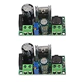
- AC/DC to DC Buck Step Down Converter Module: AC Voltage Input : AC 5V- 30V or DC 5V-50V;Output Range: DC 3.3V-33V
- LM2596HV Buck Converter: Output Current Range: Up to 2.2A (Regulator Chip Can Withstand a Maximum Current of 3A, Can Work at 3A Output Current for a Short Time)
- High Current: AC/DC to DC Buck Step Down Converter Module with External Heat Sink can Withstand High Current Operation
- High Voltage Version:Power Module Adopts the Plug-in LM2596HV, High Voltage Version of the LM2596. The Maximum Input Voltage is 50V (Limited by the Filter Capacitor Withstand Voltage)
- Input Terminal of Step Down Converter Module Uses a 4A Rectifier Bridge Stack to Input AC Power, and Has a Dedicated DC Input Port, Which is Commonly Used for AC and DC Input. The Output Voltage Can Be Adjusted from 3.3V to 33V, and the Output Voltage Will Vary with Different Input Voltage Ranges
Check capacitor losses under operating conditions
For input and output capacitors, check ESR and ESL at the operating frequency, ripple-current rating, temperature behavior, and effective capacitance under DC bias. A nominal capacitance value does not establish that the part will retain enough capacitance in circuit. Include the loss and heating associated with the actual ripple current.
Independent reader supportYour contribution helps us test, update, and keep practical guides available for everyone.Make layout and timing part of the efficiency design
Parasitic inductance and resistance can produce ringing, EMI, additional switching energy, and device stress. Fix the current paths before trying to compensate with faster edges or a higher switching frequency.
- Keep the high-di/dt switching loop compact, with short, wide current paths.
- Place input bypass ceramics directly across the switching current path and close to the switches.
- Keep the gate-drive loop short; reference the driver to the MOSFET gate and source with a clean return, using a Kelvin source connection where applicable.
- Provide adequate copper and thermal vias to carry heat away from switches and other hot components.
- After minimizing parasitics, tune gate resistance, dead time, snubbers, and clamp networks while checking switching-node ringing, EMI, and device temperature.
Dead time is a real trade-off: too much can increase diode conduction loss, while too little can risk shoot-through. Tune it for the actual devices and timing, and verify the gate and switching-node waveforms rather than relying only on nominal controller settings.
Validate efficiency across the operating envelope
- Measure input and output power. Use suitable bandwidth and probing for the converter, and calculate efficiency from measured power rather than inferring it from a component’s nominal ratings.
- Sweep line and load. Record performance at minimum and maximum input voltage and over the relevant load range, including light load and full load.
- Allow temperatures to stabilize. Record component temperatures after thermal stabilization so the comparison includes temperature-dependent resistance and heating.
- Inspect switching waveforms. Check the switch node and gate signals for voltage-current overlap, ringing, excessive dead time, or shoot-through.
- Compare with the loss budget. Investigate material differences between estimated and measured loss before increasing frequency or changing parts.
There is no defensible universal efficiency gain from raising frequency without the converter topology, voltages, components, load profile, and measurements. Keep the frequency only if the observed size or response benefit is worth its measured losses, thermal stress, EMI consequences, and cost.
Recommended Free Tools
Quick Recap
Product prices and availability are accurate as of the date/time indicated and are subject to change. Any price and availability information displayed on Amazon at the time of purchase will apply.

