
Windows Errors? Fix Them Before They Spread
Repair common Windows errors and clear accumulated junk for a smoother, more stable PC - no reinstall needed.Free scan · no reinstallOutdated Drivers Are Slowing You Down
One free scan finds every outdated or missing driver and matches the right update for your exact hardware.Free scan · exact hardware matchA “2 nm” chip is made using a process generation called 2 nm; the name does not mean its transistors, or their gates, measure 2 nanometers. IBM Research reported a 12 nm gate length in its 2021 2 nm-node demonstration—one measured dimension in that particular research device, not a universal size for 2 nm-class chips.
What does 2 nm mean in chips?
It is a label for a generation of semiconductor manufacturing technology, not a measurement of one transistor feature. IBM explains that recent names such as 10 nm, 7 nm, 5 nm, and 2 nm refer to generations of chips made using particular processes. The 2 nm label does not correspond to the traditionally defined contacted-metal half-pitch measurement. IBM Research explains its 2 nm node label.
That makes the name useful as a broad shorthand for a process generation, but not as a ruler. A foundry’s “2 nm” label does not establish that its transistor gate is 2 nm long, nor does it provide a direct physical conversion to another foundry’s node name.
Are 2 nm transistors actually 2 nanometers?
No—not on the evidence of the commonly cited IBM demonstration. IBM Research reported a 12 nm gate length for a transistor in its 2021 2 nm-node research chip. That figure describes the gate length in that specific demonstration; it is not a claim that every feature of the chip measures 12 nm, or that all 2 nm-class processes use a 12 nm gate.
The Tool Desk
Outbyte PC Repair FREERepair Windows errors before they cause bigger problemsFix Now →Outbyte Driver Updater FREEFix the driver behind crashes, sound loss and screen glitchesFind Drivers →#1 Best Overall

- CURIOSITY DEV BOARD, 32BIT, PIC32 MCUThis listing is for Each
A transistor has multiple dimensions, so asking for its single “actual size” can be misleading. Gate length is one measurement. Other useful quantities include contacted gate pitch, minimum metal pitch, transistor density, and performance or power at a stated operating point. Those measures answer different questions and should not be substituted for one another.
What transistor architecture does the 2 nm label describe?
The label alone does not specify transistor architecture. IBM’s 2021 research demonstration used horizontally stacked nanosheets with gates surrounding the channels—a gate-all-around design. IBM said its demonstration contained 50 billion transistors in an area roughly the size of a fingernail. Those are IBM’s descriptions of that research chip, not a specification that can be assumed for every product bearing a 2 nm-class label.
Rank #2

- Supports 8-, 14-, 20-pin 8-bit PIC Microcontrollers with low voltage programming capability
- Integrated Programmer/Debugger with USB
- Interface Integrates seamlessly with MPLAB X IDE and Code Configurator
- Various user interface options - mTouch button, analog potentiometer, and physical switches
- Mikrobus support with over 100 MikroElectronika Click add-on boards available
For a current production-status example, TSMC’s official logic technology page says its N2 process uses first-generation nanosheet transistors and began volume production in the fourth quarter of 2025 as planned. The information describes TSMC’s N2 process specifically; it does not make TSMC’s node name a common dimensional scale shared with other foundries. See TSMC’s Logic Technology page.
Why do foundries’ node names not compare like measurements?
Companies use process-generation names within their own technology frameworks. Intel’s July 2021 corporate announcement said that traditional nanometer-based process-node naming stopped matching actual gate length in 1997. That is Intel’s explanation of naming history, not an independent standards-body rule that converts every company’s node label into a physical dimension. Intel’s announcement provides its naming context.
Rank #3

- 2.4GHz Dual Mode WiFi + Bluetooth Development Board
- Ultra-Low power consumption, works perfectly with the Arduino IDE
- Support LWIP protocol, Freertos
- SupportThree Modes: AP, STA, and AP+STA
- ESP32 is a safe, reliable, and scalable to a variety of applications
As a result, “2 nm” from one foundry should not be treated as physically identical to “2 nm” from another. A sound comparison needs disclosed values for the same metric, defined on a comparable basis. The available figures here do not establish a complete, directly comparable table of physical dimensions across current 2 nm-class processes.
What can you compare instead of the node name?
Look for the metric that matches the question, along with the process, foundry, date, and context in which the number was reported.
Rank #4

- ❥❥❥ The PIC16F877A Microcontroller Development Board features an onboard 4M crystal oscillator, allowing easy replacement of the socket crystal frequency for various applications.
- ❥❥❥ Equipped with a 4-bit independent keyboard connected to RB0, RB1, RB2, and RB3, this board enhances interactivity and supports various input methods for your projects.
- ❥❥❥ The board includes eight LEDs connected to the RD port, operable through the J3 connector, providing visual feedback for output operations and simplifying debugging.
- ❥❥❥ With a standard RS232 communication interface, the microcontroller board facilitates seamless communication with computers, making data transfer and programming straightforward.
- ❥❥❥ The board supports external 5V DC power supply via USB, an ICSP programming simulation interface for various tools, and easy extension of all IO ports using pin headers for flexible project development.
- Gate length: the length of the transistor’s gate; IBM’s 12 nm figure is for its 2021 research demonstration.
- Contacted gate pitch and minimum metal pitch: distinct layout dimensions. Do not infer either from a node label or from gate length.
- Transistor density: compare only when the density figure and the calculation method are disclosed on a comparable basis.
- Performance or power: compare at a stated operating point. A performance-at-equal-power claim is not interchangeable with a power-at-equal-performance claim.
IBM reported approximately 45% better performance at the same power, or approximately 75% lower power at the same performance, compared with what it called “today’s 7 nm chips” in its 2021 announcement. These are IBM’s reported comparisons at that time, not independently established guarantees for current retail products. The announcement does not make those percentages a general consequence of a 2 nm label.
Independent reader supportYour contribution helps us test, update, and keep practical guides available for everyone.What the 2 nm label cannot tell you
- It does not state the gate length or any other single physical dimension.
- It does not by itself specify the transistor architecture, pitch, or transistor density.
- It does not guarantee a particular level of performance, power efficiency, or improvement over another process.
- It does not establish that two foundries’ similarly named nodes have the same dimensions.
For an accurate comparison, use matched, explicitly defined measurements from the relevant foundries. When those disclosures are not available on a comparable basis, the physical-size comparison remains unresolved rather than something that can be calculated from “2 nm.”
Quick wins for a faster PC:
Fix the driver behind crashes, sound loss and screen glitchesFind Drivers →Clear out junk files and repair common Windows errorsFree Scan →Quick Recap
Best Value
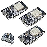
- High-performance dual-core processor – ESP32S is equipped with a powerful dual-core 32-bit CPU with a main frequency of up to 240MHz, providing smooth and efficient computing power for IoT and embedded applications.
- Wi-Fi & Bluetooth dual-mode support – Integrated 2.4GHz Wi-Fi and low-power Bluetooth, supporting wireless data transmission, remote control and smart device connection.
- Rich interfaces and functions – Provides GPIO, UART, SPI, I2C and other interfaces, supports touch sensing, infrared remote control, DAC and other functions, suitable for a variety of electronic projects.
- Low-power design – With multiple power saving modes, supports deep sleep and ultra-low power operation, suitable for battery-powered Internet of Things (IoT) devices and remote monitoring systems.
- Compatible with multiple development environments – Supports for Arduino IDE, for ESP-IDF, for MicroPython and for PlatformIO, easy to develop, suitable for beginners and advanced developers to quickly build smart applications.
Product prices and availability are accurate as of the date/time indicated and are subject to change. Any price and availability information displayed on Amazon at the time of purchase will apply.

