
iTechGuides is reader-supported. When you buy through links on our site, we may earn an affiliate commission. As an Amazon Associate I earn from qualifying purchases. Learn more
Custom memory for AI does not always mean inventing new DRAM. The approaches now under discussion instead tailor the memory stack, its base die, or the way it is attached to compute—seeking more usable bandwidth and lower data-movement costs without giving up the capacity and manufacturing advantages of established memory. Marvell’s custom HBM4E, GUC’s DRAM-on-Logic (DoL), Samsung’s SAINT-D, and research into stacking HBM above processors illustrate different points on that design spectrum. The reported figures are company claims or simulation results, not a like-for-like independent benchmark. EE Times’ March 12, 2026 report describes the designs and the manufacturing, thermal, and adoption hurdles that remain.
What does “custom memory” mean for AI systems?
It usually means adapting how memory connects to or is packaged with a processor, rather than necessarily changing the DRAM cells themselves. The goal is to move data to compute with less interface overhead, better energy efficiency, or a denser package. A design can therefore use standard DRAM while customizing the base die and the link to the processor; another can place DRAM layers directly over a compute die.
These choices address different constraints. HBM offers substantial capacity and bandwidth in a package connected alongside a processor. SRAM integrated on a compute die is closer and faster, but costly in area and limited in capacity. DRAM-on-Logic aims at a middle ground: more memory density than on-die SRAM and tighter proximity than off-package memory. None of those positions alone establishes which design is best for a particular accelerator; workload, package, cooling, software, and manufacturing yield all matter.
Outdated Drivers Are Slowing You Down
One free scan finds every outdated or missing driver and matches the right update for your exact hardware.Free scan · exact hardware matchWindows Errors? Fix Them Before They Spread
Repair common Windows errors and clear accumulated junk for a smoother, more stable PC - no reinstall needed.Free scan · no reinstallHow do the approaches compare?
The figures below are reported by EE Times from Marvell, GUC, an imec simulation, and other named sources. They are not measured under a common test setup. A dash is avoided: where the report does not give a comparable value, the cell says so.
#1 Best Overall
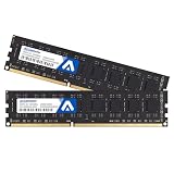
- System Upgrade: Designed for desktop PCs upgrading to DDR3-1600 (PC3-12800) memory, this upgrade maximizes memory performance through dual-channel configuration. Please check if your motherboard is DDR3 compatible before purchasing.
- Specifications: CL=11, Pin Count = 240, Dual Voltage = 1.5V, ECC Type = Non-ECC, Form Factor = Unbuffered UDIMM
- Stable Performance: High-performance memory chips, dual-in-line memory architecture, using a 512MB*16 high-performance memory chip architecture to ensure optimal performance at all times. More compatible with older motherboards/CPUs.
- DDR3 memory uses original IC chips. Compliant with RoHS and JEDEC standards, highly compatible with some desktop computers.
- Aclamator DDR3 memory modules come with a lifetime warranty and comprehensive service and technical support.
| Approach | Integration and memory | Reported performance or efficiency figures | Key qualification |
|---|---|---|---|
| Marvell custom HBM4E | Custom base die and compute-die interface with JEDEC-standard HBM4E DRAM and stack geometry. | Marvell reports up to 2.048 TB/s per custom stack; it cites 3.072 TB/s for a standard HBM4E stack. It also claims up to 25% of SoC area freed, 45%–70% lower memory-I/O power depending on scenario, and support for 33% more memory or an opportunity to lower SoC cost. | Company-reported figures; no independent like-for-like validation is provided in the report. |
| GUC DRAM-on-Logic | Four to eight customized DRAM layers hybrid-bonded above a compute die using TSMC SoIC. | GUC figures shared at a TSMC forum include up to about 5 TB/s, roughly 30 ns latency, around 0.5 pJ/bit, and 10–40 MB/mm² density depending on stack height. | Company-supplied figures; production-scale yield and pre-assembly testing remain open questions. |
| Samsung SAINT-D | DRAM-on-logic integration offered through Samsung’s foundry, packaging, and memory operations. | Not stated (EE Times, March 12, 2026). | The report provides no independent comparative performance results. |
| HBM stacked above a GPU | Three-dimensional placement puts HBM directly over the processor rather than around it in a 2.5D package. | In the cited imec simulation, the unmitigated 3D layout peaked at 141.7°C versus 69.1°C for the 2.5D layout under the same stated cooling conditions. KAIST estimated roughly 75 W dissipated by a 12-high/16-high HBM4 stack. | The temperatures are simulation results, not measurements of a shipping product; the power figure is an attributed estimate. |
Bandwidth, latency, energy, capacity, and density numbers here are not directly interchangeable: the designs and reporting conditions differ. The report does not provide a common capacity comparison, bandwidth per unit of capacity, or a complete cost comparison across all four approaches.
What is Marvell changing in HBM4E?
Marvell’s design keeps the DRAM and stack geometry within the JEDEC-standard HBM4E framework, while customizing the base die and the interface to the compute die. In other words, it changes the connection and supporting logic rather than requiring a wholly new DRAM stack. Marvell senior director of product marketing Khurram Malik described the division this way: “The customization happens in the base die and in the interface to the compute die.”
The proposed interface replaces the conventional wide HBM4 PHY on the compute die with a proprietary 512-bit bidirectional die-to-die link. Marvell’s case is that this could free processor area and reduce memory-I/O power while retaining standard DRAM. The trade-off is that the custom interface and base die are still part of the system design: standards-compliant memory does not make the entire solution interchangeable with a conventional HBM implementation.
The Tool Desk
Outbyte PC Repair FREERepair Windows errors before they cause bigger problemsFix Now →Outbyte Driver Updater FREEScan for outdated or missing drivers - takes under a minuteDriver Scan →Rank #2

- Simple design to perfectly protect the cooling module
- High thermal conductive adhesive
- Supports Intel & AMD motherboards
- Selected high-quality IC, Supports XMP2.0
- Lifetime warranty
Where does DRAM-on-Logic fit?
GUC positions DoL between on-die SRAM and off-package HBM for workloads that benefit more from bandwidth than from the very large capacity of conventional HBM configurations. Its design uses hybrid bonding to attach multiple customized DRAM layers directly above compute logic, a tighter integration than placing memory beside the processor.
That closeness can shorten data paths, but it joins manufacturing processes and structures that must align precisely. Michael Schuette, CTO of DataSecure and CTO/chief scientist of Boolean Labs, told EE Times: “But you are looking at two different manufacturing processes, and the smaller the geometry, the more difficult it gets to align the different blocks.” GUC’s reported performance figures should therefore be read alongside the unresolved questions about yield at higher production volumes and whether DRAM layers can be tested individually before bonding. Those issues affect cost and the ability to isolate a defective layer or assembly.
What is Samsung’s SAINT-D platform?
SAINT is Samsung’s 3D integration platform, with SAINT-S for SRAM-on-logic, SAINT-L for logic-on-logic, and SAINT-D for DRAM-on-logic. The report describes SAINT-D as flexible enough to use custom DRAM, HBM, or commodity DRAM, rather than tying the platform to only one memory type.
Rank #3
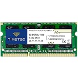
- [Specs] DDR3L / DDR3 1600MHz PC3L-12800 / PC3-12800 204-Pin Unbuffered Non ECC 1.35V CL11 Dual Rank 2Rx8 based 512x8
- [Size] Module Size: 8GB Package: 1x8GB
- [Voltage] JEDEC standard 1.35V, this is a dual voltage piece and can operate at 1.35V or 1.5V
- [Compatibility] Compatible with DDR3 Laptop / Notebook PC, Mini PC, All in one Device
- [Color] PCB Color is Green
Samsung’s potential advantage is organizational as much as architectural: its turnkey offering combines foundry, advanced-packaging, and memory operations. Bringing those capabilities together may simplify coordination between components of a package, but the report does not establish a performance lead or quantify a manufacturing advantage for SAINT-D.
Why is HBM above a processor so difficult to cool?
HBM4’s wider interfaces increase connection complexity, but placing memory directly over a processor creates a separate problem: heat from the logic has a harder path out of the package, while the memory stack itself also dissipates heat. The resulting thermal resistance can force compromises in clock speed, workload throughput, or package cooling. Rambus fellow and distinguished inventor Steven Woo summarized the scaling concern to EE Times: “Thermal management, power delivery, and yield issues make such integration difficult at scale, especially as both logic and memory densities increase.”
The cited imec work examined ways to mitigate heat in a simulated 3D configuration, including reducing GPU frequency, merging HBM stacks, and double-sided cooling. Imec system technology program director James Myers said the frequency-reduction step carried a 28% workload penalty—described as a slowdown of AI training steps—while the overall package in the discussed configuration outperformed the 2.5D baseline because of higher throughput density. That is a result for the simulation and configuration in question, not a general guarantee that 3D packaging will outperform 2.5D systems.
Rank #4

- [Color] PCB color may vary (black or green) depending on production batch. Quality and performance remain consistent across all Timetec products.
- DDR3L / DDR3 1600MHz PC3L-12800 / PC3-12800 240-Pin Unbuffered Non-ECC 1.35V / 1.5V CL11 Dual Rank 2Rx8 based 512x8
- Module Size: 16GB KIT(2x8GB Modules) Package: 2x8GB ; JEDEC standard 1.35V, this is a dual voltage piece and can operate at 1.35V or 1.5V
- For DDR3 Desktop Compatible with Intel and AMD CPU, Not for Laptop
- Guaranteed Lifetime warranty from Purchase Date and Free technical support based on United States
Why have earlier processing-in-memory designs not taken over?
Processing-in-memory (PIM) tries to reduce energy and time spent moving data by performing some operations close to, or within, memory. The idea is attractive for data-heavy workloads, but proximity alone is not enough to displace a general-purpose accelerator.
EE Times points to efforts including Micron’s Automata Processor, Samsung HBM-PIM, and SK Hynix GDDR6-AIM. Its analysis is that these efforts faced narrow workload targets and could not match mainstream GPUs’ mature software ecosystems and economics. Adoption also depends on whether developers can program the hardware, whether it fits into existing systems, and whether the workloads recur often enough to justify specialized silicon. Memory makers’ business incentives matter too: a technically elegant design may not be compelling if it requires a new product ecosystem without a clear commercial return.
What should buyers and system designers take away?
- Look beyond peak bandwidth. Capacity, latency, energy per bit, cooling, and usable throughput for the target workload all affect system value.
- Separate memory standards from package customization. A design may retain standard DRAM while still requiring a proprietary interface, custom base die, or specialized assembly.
- Ask how defects are found and handled. Testing access, yield, and repair or replacement options become more consequential as layers are bonded into a package.
- Check software fit and economics. A specialized memory architecture needs supported tools and a sufficiently large workload advantage to justify integration complexity.
The approaches are not a single contest with a clear winner. Marvell is customizing the HBM connection while preserving standard HBM4E DRAM; GUC and Samsung are exploring DRAM-on-logic integration; and direct HBM-over-GPU stacking highlights the thermal cost of tighter proximity. Which path makes sense depends on the workload and whether its system-level gains survive the realities of cooling, manufacturing, testing, and software support.
Quick Recap
Product prices and availability are accurate as of the date/time indicated and are subject to change. Any price and availability information displayed on Amazon at the time of purchase will apply.

