
Do these 3 things before closing this tab:
1Fix the driver behind crashes, sound loss and screen glitches2Repair Windows errors before they cause bigger problems3Scan for outdated or missing drivers - takes under a minuteThere is no single best nanoscale chemical imaging technique for semiconductor inspection. Choose by the unknown you need to resolve—such as a surface contaminant, a buried interface, a trace dopant, or three-dimensional device chemistry—and by the output you need: elemental identity, chemical state, molecular fragments, concentration, or a spatial map. APT, SIMS, electron microscopy and surface-analysis methods answer different questions; specimen preparation, artifacts and quantification can matter as much as nominal resolution.
Start with the question, not the instrument
Before selecting a method, define what is unknown and where it is located. “Find contamination” is not yet a measurement specification: the contaminant might be on the exposed surface, within an ultrathin film, at a buried interface, or distributed through a device volume. Those locations call for different ways of exposing and measuring the material.
Also name the result you need. Elemental identity is different from chemical state; a molecular-fragment signal is different from a quantitative concentration; and a two-dimensional cross-section is different from a three-dimensional reconstruction. ISO/TR 14187:2020, Surface chemical analysis — Characterization of nanostructured materials, emphasizes defining the required information and accounting for specimen handling and stability, probe effects, environment, and interpretation.
| Inspection question | Methods to consider | Key qualification |
|---|---|---|
| Where are dopants or trace elements in three dimensions? | Atom probe tomography (APT) | Its sensitivity and spatial mapping are powerful, but results depend on specimen geometry, evaporation behavior, and reconstruction. |
| What is at a surface or in an ultrathin layer, and how does it vary with depth? | SIMS, including ToF-SIMS | Sputtering alters the material; interpretation and quantification can depend on the matrix and method. |
| What is the localized composition of a prepared cross-section? | TEM/STEM with EDS or EELS | Preparation and complex device geometry can affect what region is measured and how results are interpreted. |
| What is the three-dimensional architecture of a complex device? | Electron tomography; APT for some compositional questions | Tomography reconstruction can introduce artifacts, so validate that the requested quantity is supported. |
| Is the exposed surface contaminated, or what is its chemical nature? | XPS, AES, or SIMS | A surface measurement does not by itself establish the composition of buried or bulk material. |
Which technique can map dopants or trace impurities?
APT for three-dimensional atomic-scale composition
APT is a candidate when you need a three-dimensional map of elemental composition or dopant distribution at very small scales. NIST describes sub-nanometer spatial resolution and sensitivity in the parts-per-million range in some cases; these are stated APT capabilities, not a guarantee for every semiconductor material or stack. NIST identifies applications including dopant profiles, composition, interfacial roughness, nucleation and clustering, diffusion, and adhesion.
Free tools Windows power users keep installed
One-click scans. No signup required.
#1 Best Overall

- Inspect Coins, Circuits & Skin Close Up: Hold this 10X-200X handheld USB-C microscope up to your phone, Android, or PC. The manual focus wheel and 8 adjustable LED lights reveal tiny details on coins, circuit boards, jewelry, and skin pores — no app needed for basic viewing.
- Manual Focus Zoom with Full Control: Unlike auto-focus scopes that hunt for the target, the precision focus wheel lets you lock onto exactly what you want to see — from 10X wide views to 200X close-ups of electronic components, stamps, and gemstones.
- 8 LED Lights with 3 Brightness Levels: The adjustable ring light eliminates shadows and glare. Turn the dial on the cable to switch between dim for shiny surfaces and bright for dark crevices — perfect for inspecting inside electronics or examining skin.
- Rotating Metal Stand for Hands-Free Use: The chrome-plated metal arm and weighted base hold the camera steady while you work. Rotate 360° to view flat documents, curved coins, or vertical circuit boards without juggling the scope.
- Complete Kit for Hobbyists & Professionals: Includes ear specula for safe ear exams, protective covers for hygiene during pet/skin checks, and side-view mirror for hard-to-reach areas. Ideal for collectors, jewelers, electronics repairers, educators, and home inspectors.
Its limitations are important in semiconductor structures. NIST documents challenges including specimen fracture, difficult interfaces, reconstruction uncertainty, and problems obtaining desired information from some advanced materials and integrated devices. Examples include incorrect high-k dielectric stoichiometry, oxide interfaces, and buried metal layers. Before committing a valuable device region, ask the laboratory whether the specific material stack and geometry have been analyzed reliably, and how it will assess reconstruction and representativeness.
SIMS when trace chemistry or a depth profile is the target
SIMS measures ions produced from a surface under ion bombardment. ToF-SIMS can provide elemental and molecular-fragment information from the near-surface region; sputtering can expose successive material and produce a depth profile. PHI describes its TOF-SIMS technique as having an approximately 1 nm average analysis depth and less than 0.1 µm ultimate spatial resolution. These are vendor statements about PHI instruments, not universal specifications or a direct comparison with every other instrument.
Rank #2
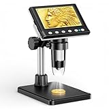
- 🔍【Precision Detail Inspection for Hobbyists】 Designed specifically for coin collectors, jewelers, and watchmakers requiring extreme close-ups. While the 4.3-inch screen is optimized for localized high-magnification rather than full-coin viewing, it flawlessly captures microscopic mint errors, dates, and intricate jewelry textures with its 1000X HD resolution.
- 📺【Compact Standalone Observation System】 Experience instant plug-and-play convenience for all your hobby explorations. The integrated 4.3-inch LCD display eliminates the need for software, Wi-Fi, or external monitors, offering a space-saving footprint that is ideal for crowded workbenches or on-the-go appraisal sessions.
- 💡【Anti-Glare Illumination for Reflective Surfaces】 Inspect glossy coins, polished watch dials, and metallic jewelry without blinding reflections. Equipped with 8 dimmable LED ring lights, the smooth brightness control wheel ensures even, shadow-free clarity, allowing you to reveal the finest surface conditions under any ambient lighting.
- 🛠️【Stable Focusing for Micro-Components】 Achieve sharp, jitter-free imaging during delicate watch repairs or diamond appraisals. The weighted base and smooth rotary focus wheel provide precise distance control, empowering users to effortlessly lock in the exact magnification needed from 50X to 1000X without screen shaking.
- 🎁【Complete Starter Kit with Clear Instructions】 Start your microscopic journey immediately with all essential accessories included, featuring the dedicated charging cable and user manual. Note: The lens features a pre-installed clear protective cover designed to prevent shipping scratches, which must be removed prior to use for crystal-clear results.
Because sputtering removes or alters material, the profile is not a nondestructive view of an untouched specimen. Ask how the laboratory handles matrix effects, calibrates or quantifies the target species, and distinguishes genuine interface behavior from sputter-related effects. For higher-resolution SIMS imaging in materials science, a 2020 Annual Reviews review describes spatial resolution of 50–100 nm in the context of light-element detection and isotope/isobar separation; that review figure is not a universal SIMS specification.
How do APT, ToF-SIMS, and STEM-EDS differ?
These methods are not interchangeable ways to obtain one generic “chemical image.” Their useful outputs and sampling approaches differ:
Rank #3

- 4.3 Inch LCD Digital Microscope with High Definition and Convenient Focusing: Electronics microscope has 1000 times magnification and 1080p / 720p resolution. Adjust the object to the lens and slowly turn the focusing wheel to see the fine details. It has a built-in rechargeable lithium battery, which can work for 4-5 hours. It is portable and independent with enough power for outdoor observation and can be used by hand without the bracket
- 50X-1000X Digital Magnification Range: LCD digital microscope has 2.0MP camera technology and precise focus. The microscope magnification is 50X to 1000X, allowing you to clearly view the smallest details of the specimen, such as plants, coins, diamonds, and welding, helping you easily see the clear details of tiny objects
- 4.3-Inch High-Definition LCD Screen with 32GB Storage Card: 4.3-inch screen microscope can capture a clear detailed view of the object in a certain area of the picture and record video, documenting a clear micro-world experience. The images and videos obtained during the observation process are saved in a 32GB SD micro card (Included 32 microSD card)
- 8 Adjustable LED Lights for Optimal Illumination: Microscope has built-in 8 adjustable LED lights. The brightness can be adjusted from dark to bright by sliding the switch, providing excellent details and best definition to improve the quality and clarity of user images and videos
- Easy to Adjust Focus Function with Metal Bracket: Adjust the object close to the lens, and then slowly rotate the focus wheel to clearly view the sample on the 4.3-inch screen. The attached metal bracket can be used for stable shooting and hands-free operation
| Method | Best-aligned output | What to check before analysis |
|---|---|---|
| APT | Three-dimensional atomic composition or dopant distribution | Whether the stack can be prepared and measured without fracture or misleading reconstruction; whether the sampled volume represents the feature of interest. |
| ToF-SIMS | Surface or near-surface species, molecular fragments, and sputter-based depth distributions | Target-specific sensitivity, matrix effects, sputter damage, depth calibration, and quantitative method. |
| STEM-EDS | Localized elemental information aligned with a prepared cross-sectional structure | Cross-section preparation, spatial resolution and detection limits for the elements of interest, and whether the section intersects the suspected defect. |
PHI contrasts typical SEM/EDS analysis depth of 1–3 µm with TOF-SIMS analysis depth typically below 2 nm. This is a vendor comparison and should not be treated as a universal instrument-to-instrument benchmark; actual sampling depends on the instrument and operating conditions. It illustrates why a surface-sensitive measurement and electron-based analysis of a prepared cross-section may see different parts of the same device.
What can analyze a buried interface or complex device?
Cross-sectional TEM/STEM with spectroscopy
When the question is localized chemistry alongside device structure, TEM or STEM combined with EDS or EELS is a natural candidate. Electron microscopy and spectroscopy can connect a prepared cross-section with local structure and composition. JEOL documents semiconductor application examples including cross-sectional elemental mapping and chemical-state analysis; those are vendor applications, not an independent performance comparison.
Rank #4

- SUPER widefield optical system offering sharp erect stereo images
- SUPER widefield optical system offering sharp erect stereo images
- SUPER widefield optical system offering sharp erect stereo images
- 2-1/2" (65mm) SUPER widefield view and 8" (200mm) large working distance
- XL pillar stand and X-Y gliding table for easy object control
The required cross-section must expose the feature of interest. Preparation can be demanding, and a small section may not represent a heterogeneous device or an extended defect. Specify the location and suspected feature with the laboratory, and ask how it will verify that the section includes the relevant interface or failure site.
Electron tomography for three-dimensional architecture
If the unknown is the three-dimensional shape or arrangement of structures, electron tomography may be relevant. NIST describes active work on quantitative 3D electron-tomography methods because complex semiconductor architectures challenge existing imaging. Reconstruction artifacts can limit quantitative conclusions, so ask whether the laboratory has validated the requested measurement—not merely whether it can produce a 3D rendering.
Best Value
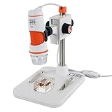
- 20X–200X MAGNIFICATION WITH PROFESSIONAL-QUALITY OPTICS: 5-element IR-cut glass lens delivers crisp, detailed views of coins, circuit boards, textiles, insects, and more.
- TRUE 5MP DIGITAL SENSOR: Capture stunning, high-resolution images (up to 2592 x 1944 pixels) and VGA-quality video for sharing, analysis, or archiving.
- BUILT-IN POLARIZING FILTER: Reduce glare and reflections on shiny or wet surfaces with the adjustable polarizing filter wheel for clearer, more detailed views.
- CONVENIENT ONE-TOUCH SNAPSHOT BUTTON: Press the button to capture images anytime without touching your computer.
- USB-C CONNECTIVITY + LONGER CABLE: Plug-and-play connection to Windows and Mac computers with an over 4-foot USB-C cable.
Which surface-analysis method fits contamination or thin films?
XPS and AES for surface chemistry
X-ray photoelectron spectroscopy (XPS) and Auger electron spectroscopy (AES) are options when the question concerns exposed-surface composition or chemical nature. ISO/TR 14187:2020 identifies both among surface chemical-analysis approaches and notes that such analysis can address contamination, coating thickness, and surface chemistry before or after processing. The measurement may not describe buried bulk material; sample handling, stability, environment, probe effects, and interpretation need to be considered.
SIMS for surface species and depth variation
Choose SIMS when detecting surface or near-surface species, molecular fragments, or their variation with sputtered depth is central. For an ultrathin layer, confirm the laboratory’s effective sampling depth and depth resolution under the proposed conditions rather than applying a vendor figure as a universal guarantee. If a buried interface must be investigated, plan how the overlying layers will be removed or exposed and how that preparation could affect the result.
How to choose and brief an analysis laboratory
- State the unknown and its location. Specify the target species or property and whether it is expected at the surface, in a thin film, at an interface, or within the device volume.
- Define the deliverable. Say whether you need elemental identity, chemical state, molecular fragments, concentration, a depth profile, a 2D map, or a 3D reconstruction.
- Set scale and sensitivity requirements. Identify target elements and the detection limit, lateral scale, sampling depth, and uncertainty needed to make the process or failure decision.
- Discuss the exact specimen and preparation. Ask what region must be exposed, whether the measurement is destructive, what preparation risks exist, and whether the analyzed region can represent the integrated device.
- Request method-specific evidence. Ask about calibration or quantification, relevant standards, matrix effects, known artifacts, repeatability, uncertainty, and validation on similar materials.
- Decide whether to combine methods. A broad surface or depth profile can be paired with targeted cross-sectional electron microscopy when the failure hypothesis requires both chemical distribution and structural context.
These questions reflect measurement issues emphasized by NIST and ISO: the chosen probe and specimen handling can affect the result, while method limitations and interpretation shape what can be concluded. Do not choose on nominal resolution alone.
When to use a contract analysis provider
If your organization does not have the instrument or specialist expertise, a contract laboratory may offer a practical route. SGS USA lists semiconductor material-analysis services including AFM, TEM, EDX, XPS, AES, SIMS, ToF-SIMS, and dynamic SIMS. A published service menu does not establish that a particular location currently offers a method, can analyze your exact stack, or meets a required detection limit. Confirm regional availability, sample requirements, deliverables, and capability directly. JEOL’s semiconductor application material can also help identify relevant instrument approaches, but application examples are not proof of a specific service capability.
Recommended Free Tools
Quick Recap
Product prices and availability are accurate as of the date/time indicated and are subject to change. Any price and availability information displayed on Amazon at the time of purchase will apply.

