
Quick wins for a faster PC:
Fix the driver behind crashes, sound loss and screen glitchesFind Drivers →Clear out junk files and repair common Windows errorsFree Scan →Reducing RF coupling in a wireless system-on-chip (SoC) requires controlling several paths at once: electromagnetic coupling between routes and inductors, noise carried through shared power and ground impedances, and conductive coupling through the substrate. Start with floorplanning and routing, then add process-supported isolation and shielding where needed. Finally, verify the complete design with extracted coupling models and measurements of both coupling and RF-block performance; no single isolation technique works equally well across frequencies, geometries, substrates, and packages.
Identify the path before choosing an isolation technique
RF interference can travel through more than one route. A mitigation aimed at the substrate, for example, will not by itself remove magnetic coupling between adjacent inductors or noise conducted through a shared supply. Electronic Design’s Karim Saleh and Mohammed Tawfik AbdelHafez identify radiated electromagnetic interference, magnetic coupling between routes and coils, substrate coupling, and domain-to-domain signal transfer as issues in wireless SoC design (March 19, 2025).
- Electromagnetic and magnetic coupling: Fields from an RF structure or switching route can couple into a nearby sensitive route or passive component. Inductors are especially important to consider because their fields and the geometry of nearby conductors affect coupling.
- Shared supply and ground impedance: Digital switching current flowing through impedance shared with an RF block can create voltage disturbances in the RF block. This is a conducted path, so moving signal wires alone may not solve it.
- Substrate coupling: Noise can propagate through the semiconductor substrate between blocks. Its severity depends on factors including frequency, separation, and substrate material.
- Inter-domain signal transfer: Signals crossing between digital and RF-related domains can carry switching activity or inject disturbances at the receiving boundary.
Make an aggressor-and-victim map before selecting fixes: list likely noise sources, sensitive RF nodes, their physical proximity, and possible shared supply, ground, and substrate paths. A block can have several meaningful coupling paths at once.
Use floorplanning and routing as first-line controls
Separate sensitive routes from noisy structures
Keep sensitive RF routes away from inductors, high-activity digital routes, and other plausible aggressors where the floorplan allows. Apply separation to the actual sensitive nets and noisy structures, not just to block outlines: a nominal gap between blocks is less useful if a noisy route still passes beside an RF input.
Free tools Windows power users keep installed
One-click scans. No signup required.
#1 Best Overall
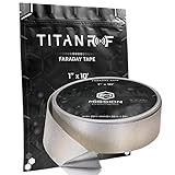
- ✅ FLEXIBLE AND DURABLE FARADAY TAPE - Extremely high-shielding conductive adhesive tape with peelable backing will not rip or tear without strong force or scissors.
- ✅ MULTIPLE APPLICATIONS - Used for industrial (military, construction company, IOT developer), or DIY (consumer) EMI/RF shielding equipment, components, cages and enclosures.
- ✅ LAB TESTED & CERTIFIED - IEEE 299-2006 shielding effectiveness confirmed with full test report, available upon request.
- ✅ EASY TO USE - Simplest way to repair a punctured faraday bag or connect multiple sheets of TitanRF Faraday Fabric. Includes instruction card for common uses.
- ✅ 1 INCH x 10 FEET - Full roll measuring 1in wide x 10ft long (2.54cm x 3.05m). Multiple size variations available.
Reduce magnetic coupling with route orientation
Where practical, route coupled or nearby conductors orthogonally rather than parallel to reduce magnetic coupling. This is a layout measure, not a substitute for checking coupling in the actual geometry. The effect depends on the structures and their separation.
Plan returns and grounds along with signal paths
Account for the return-current path and shared impedance when arranging supplies and grounds. Saleh and AbdelHafez recommend bulk ties that provide low-impedance paths to separate ground pads. Whether that approach is available and effective depends on the process and implementation; check the PDK and the extracted power, ground, and substrate network rather than assuming a ground connection is ideal.
Rank #2

- Strong Adhesive - Kirecoo copper tape [2inch, 33FT], The copper foil tape conductive adhesive is super sticky and is protected with an easy peel backing which make it can be used on most surfaces & is able to withstand all weather conditions.
- Highly Conductive - Our copper foil uses a highly conductive material with low resistance, has dual conductivity so current will flow through both sides and the adhesive. No need to worry that the copper tape conductive adhesive will reduce the effectiveness between components, making our emi shielding foil a excellent option for electrical projects, repairs and even paper circuits. Excellent alternative to conductive paints.
- EMI & RFI Shielding - This copper foil tape with conductive adhesive Shielding electric guitar to avoid interference, shield the pickup and control cavities of a guitar. Prevent radiating and interfering, making it an ideal guitar shielding tape option. Perfect for any guitar builder/ luthier.
- Good helper for gardening - This copper tape can for slugs. You can wrap copper tape around the base of small plants Works for keeping slugs & snail away! Seedlings to protect plants. This was the perfect eco friendly solution!
- Creative Decoration - Our copper tape is a desirable choice for decorating your home, making personalized wall vinyl’s, jewellery, stainless glass & more that will come in handy for various DIY & Creative projects. Also perfect for solder, birthday light card, paper circuit or repair such as LCD monitor mobile phone.
Choose isolation measures for the process and the RF block
Deep N-wells, high-resistivity regions, SOI buried oxide, guard rings, and patterned ground shields can reduce some forms of coupling, but they have different physical effects and costs. Compare them against the coupling path you need to control and the impact on RF performance, area, integration, and verification.
| Technique | Potential benefit | Tradeoffs and design checks |
|---|---|---|
| Deep N-well | Can isolate circuits within a bulk CMOS implementation. | Effectiveness is geometry- and process-dependent. Check PDK support, area, parasitics, and latch-up or integration constraints. |
| High-resistivity substrate or native layer | Can lower substrate coupling and improve RF passive performance. | Results depend on substrate material, frequency, distance, and integration. High-resistivity material can present latch-up and integration tradeoffs for digital blocks. |
| SOI buried oxide | The buried oxide beneath active transistors suppresses substrate coupling between blocks and reduces parasitic capacitance. | Availability and suitability depend on the process and design. RF-SOI is used for RF front-end switches from sub-1 GHz through millimeter-wave applications, but this does not make it a universal replacement for bulk CMOS. |
| Guard rings | Can provide isolation paths around circuit regions. | Effectiveness depends on width, frequency, available area, and required attenuation. Confirm grounding and geometry in the intended process. |
| Shield or patterned ground shield | Can intercept fields; slots in a patterned ground shield can interrupt closed eddy-current loops beneath inductors. | A shield can add parasitic capacitance by terminating signal fields on itself. Its series resistance becomes more damaging as frequency rises; assess effects on inductor Q and phase noise. |
IEEE’s RF CMOS review discusses high-resistivity substrates, latch-up, and well-to-well isolation (published March 31, 2003; DOI 10.1109/TED.2003.810470). The IEEE Technology Navigator describes the buried oxide in SOI and its role in suppressing substrate coupling and parasitic capacitance, as well as RF-SOI use in front-end switches. These process-level descriptions are not guaranteed isolation figures for a particular SoC: validate any option against the foundry’s process documentation and design rules.
What’s actually slowing this PC down?
Pick the symptom - the matching free tool is one click away.
Rank #3
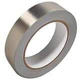
- Professional Grade: Conductive cloth tape is made of high-strength polyester fiber fabric and acrylic adhesive with a copper-nickel conductive layer formed by a special electroplating process. It ensures reliable electrical conductivity and superior electromagnetic interference shielding.
- Excellent Features: Faraday tape has good initial adhesion, with its double-sided conductive properties enabling reliable circuit connections for non-solderable electronic components. The tape also features anti-interference, anti-static, high temp resistance, and tensile strength that ensure durable performance in extreme temperatures.
- Farewell Interference: Military-grade shielding effectively blocks and suppresses external signal interference, protecting precision components from EMI and RFI. It resolves electromagnetic leakage and signal crosstalk issues, ensuring long-term stable operation of equipment.
- Multiple of Uses: Ideal for repairing internal shielded layers in devices, conduct electricity, electric repairs, electrostatic grounding, cable shield, creating paper circuits, RFID blocking, PCB heat dissipation, EMP proof, guitar noise elimination, car wire harnesses wrap, and sealing Faraday cages.
- Package Included: The full-roll conductive sticky tape measures 1" in wide × 50 Feet in length. It securely adheres to various surfaces including metal, plastic, foam, and glass, and more, while leaving no residue after removal.
Do deep N-wells and guard rings work at GHz frequencies?
They can contribute to isolation, but there is no general GHz-frequency guarantee in the cited material. Guard-ring effectiveness depends on width, frequency, area, and target attenuation; deep N-well isolation also depends on process, geometry, and the relevant coupling path. Use extracted, frequency-dependent models and measurements to establish whether the implementation meets the design’s requirement.
Control noise crossing digital-to-RF boundaries
For inter-domain connections, differential signaling can reduce noise transfer compared with a single-ended connection when the interface is implemented appropriately. For high-speed CMOS clocks and buses, Saleh and AbdelHafez recommend deliberately weakening boundary drivers to limit noise transfer. These are targeted design measures: evaluate signal integrity, timing, loading, and receiver behavior alongside their noise benefit rather than applying a weaker driver indiscriminately.
Rank #4
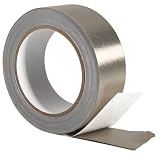
- Professional Grade: Conductive cloth tape is made of high-strength polyester fiber fabric and acrylic adhesive with a copper-nickel conductive layer formed by a special electroplating process. It ensures reliable electrical conductivity and superior electromagnetic interference shielding.
- Excellent Features: Faraday tape has good initial adhesion, with its double-sided conductive properties enabling reliable circuit connections for non-solderable electronic components. The tape also features anti-interference, anti-static, high temp resistance, and tensile strength that ensure durable performance in extreme temperatures.
- Farewell Interference: Military-grade shielding effectively blocks and suppresses external signal interference, protecting precision components from EMI and RFI. It resolves electromagnetic leakage and signal crosstalk issues, ensuring long-term stable operation of equipment.
- Multiple of Uses: Ideal for repairing internal shielded layers in devices, conduct electricity, electric repairs, electrostatic grounding, cable shield, creating paper circuits, RFID blocking, PCB heat dissipation, EMP proof, guitar noise elimination, car wire harnesses wrap, and sealing Faraday cages.
- Package Included: The full-roll conductive sticky tape measures 2" in wide × 50 Feet in length. It securely adheres to various surfaces including metal, plastic, foam, and glass, and more, while leaving no residue after removal.
Measure the tradeoffs instead of ranking techniques universally
Isolation is not one number that applies to every frequency or layout. Compare candidate measures using the conditions relevant to the design:
- Isolation effectiveness across the operating frequency range.
- Area and any routing or floorplanning constraints.
- Added parasitic capacitance and shield resistance.
- Effects on inductor Q and phase noise.
- Process availability, PDK support, and integration requirements.
- Latch-up and reliability behavior.
- Grounding complexity and the cost of verification.
For perspective on why results must be scoped, IEEE Electron Device Letters studies published in 2025 report measured glass-core test-vehicle results: 20 dB noise suppression at 40 GHz, 35 dB suppression at 60 GHz with guard rings, and a 40 dB reduction at 60 GHz with guard trenches. These measurements describe those glass-core test vehicles, not universal performance figures for on-die isolation or other substrate and package types.
Best Value

- Industrial Grade Material : Faraday Cloth Tape Two sided conductive material made up of conductive glue and conductive cloth,two sided conductive material made up of conductive glue and conductive cloth, this allows any overlapping seams of tape to be electrically continuous.Suitable for all kinds of electronic products and appliances.Applications with Faraday Conductive Tapes,metallized surface nickel, copper form excellent electrical conductivity,which not only provides stable electrical conductivity, but also has excellent shielding effect against electromagnetic interference.
- Farewell Interference: Faraday Fabric Tape, metallized surface nickel, copper form excellent electrical conductivity, used for shield electromagnetic signals and radio waves, it will reflect, absorb or penetrate according to the nature of the object, providing excellent shielding effect. It has high shielding, electrically conductive, anti-interference, radiation protection, antistatic, anti-aging, flexibility, abrasion resistance, and other properties.High Shielding Conductive Tape, suitable for a variety of surface applications, such as metals, aluminum, plastics, glass, copper / brass, and more, strong practicability, wide range of applications.
- Widely Used: Multi-purpose cloth adhesive tapes can be used for circuit connections, electrical repairs, wire interference shielding, automotive wiring harness wrap, cable fixing, creating paper circuits, PCB heat dissipation, electric guitar noise eliminate, display repair, RFID signal blocking, making conductive foam strips, electrostatic grounding, building Faraday cage and boxes, make credit card wallets, DIY projects and more.
- Wide range application: Suitable for laptop, mobilephone, lcd, pop cable, speaker, microphone, remoter, keyboard repair. EMI Shielding. Guitar interference shielding. ESD Grounding, sealing, Waterproof material. Fasten joint of pipes of airconditioner, refrigerator, packing or wraping of the data cables etc. Also can be used as circuit sticker.
- Package Included: The whole roll of conductive fabric tape is wide 2 inch/5.08cm by long 59 feet/18m. It's easy to use and residue-free, and you can cut it into round, square, bar, sheet, or other shapes to suit your needs, making it easy to apply to a wide range of sensitive parts without the need for complex tools or skills.
Build a coupling validation workflow
- Estimate likely aggressors and victims before layout. Map noisy digital domains, sensitive RF nodes, inductors, and possible shared supply, ground, and substrate paths.
- Apply layout and boundary controls. Prioritize separation and route orientation, then assess grounding, inter-domain signaling, and boundary-driver strength.
- Extract the coupling network. Include relevant interconnect, supply, and substrate coupling in signoff simulations; do not treat an ideal ground or block boundary as proof of isolation.
- Measure coupling where practical. Use S-parameters and noise-transfer measurements to characterize the implemented structures. An IEEE BCTM paper, “On-chip RF Isolation Techniques,” describes network-analyzer S-parameter measurements of coupling between adjacent inductors.
- Check the RF function, not only the isolation path. Assess consequences in block-level metrics such as phase noise, noise figure, sensitivity, linearity, and spur levels.
- Correlate models and measurements. IEEE work has modeled and measured digital switching noise degrading CMOS low-noise amplifier performance. Use relevant measured behavior to validate the assumptions in the design’s coupling models.
The result to sign off is the behavior of the RF design under realistic coupling conditions—not merely the presence of a guard ring, a shield, or an isolation layer.
Quick Recap
Product prices and availability are accurate as of the date/time indicated and are subject to change. Any price and availability information displayed on Amazon at the time of purchase will apply.

