
KiDoom turns a PCB editor into an unconventional DOOM display: copper tracks draw the walls, while component footprints stand in for enemies and pickups. The game does not run inside KiCad. Its engine runs separately, and KiCad renders the geometry it receives.
What “trace routing” has to do with DOOM
The title is a PCB-design pun. In Nick Bild’s Hackster article, the idea is framed with two questions: what if DOOM’s walls were actual PCB traces, and what if enemies and health packs were component packages? Michael Ayles’s KiDoom project turns that conceit into a software demonstration.
In the PCB Editor view, copper tracks represent walls. Footprints mark objects in the scene: Ayles uses QFP-64 footprints for enemies, SOIC-8 footprints for decorations, and SOT-23 footprints for collectibles. These package assignments are visual choices made for KiDoom, not recommended PCB-design conventions.
How KiDoom draws the scene
The game engine runs outside KiCad
DOOM is not executing as a KiCad plugin. Ayles describes the engine as a separate C process that sends vectors over a socket; KiCad is the display renderer. The project extracts wall and sprite geometry from DOOM’s drawsegs[] and vissprites[] arrays, serializes that geometry as JSON over a Unix socket, and uses Python to update PCB objects in place. Ayles summarizes the division of labor this way: “KiCad is only the display renderer. The actual DOOM engine runs as a separate C process, sending vectors over a socket.” (Ayles’s KiDoom project write-up.)
Free tools Windows power users keep installed
One-click scans. No signup required.
#1 Best Overall
![EGSCST [2 Pack] SMD Soldering Practice Kit, SMT Components Solder Training Kits for Electronics, PCB Board Soldering Practice for Beginners and Adults, DIY Electronic Project](https://m.media-amazon.com/images/I/51PazW2iQpL._SL160_.jpg)
- 【EGSCST 2-Pack Double Value】This value set includes 2 complete soldering practice kits. Having two sets allows beginners to learn from the first attempt and achieve perfection on the second board. It is the most cost-effective solution for solder training and repetitive skill-building.
- 【Professional SMT Components Training】Each EGSCST soldering kit features a wide variety of SMD components, including 0805, 0603, Diode, Transistor,and IC chips. This electronics practice kit is designed to help you master surface mount technology, moving you from basic to advanced soldering skills.
- 【High-Quality PCB with Clear Markings】Our practice soldering board is made of high-grade green PCB, featuring clearly labeled footprints for every component. This PCB soldering kit ensures that even beginners can easily follow the layout and improve their soldering accuracy with confidence.
- 【Advanced Electronic Kit for Adults】Perfect for adults, hobbyists, and students, this EGSCST soldering project offers a real-world challenge. Unlike basic kits, these advanced electronic project kits simulate professional circuit board assembly, making it an essential training tool.
- 【Essential Soldering Starter Kit】Whether you are an aspiring electrician or a DIY enthusiast, this solder project kit provides an excellent hands-on learning experience. Each of the 2 sets is a perfect addition to your laboratory bench or home workshop for learning electronics.
Three ways to view it
The project describes three views: an SDL gameplay window, a Python wireframe renderer for reference and debugging, and the KiCad PCB view used for the demonstration. KiCad is therefore one rendering option in a pipeline, rather than the place where the game logic lives.
Why use vectors instead of pixels?
Ayles says his initial pixel-by-pixel concept managed approximately 0.15 FPS. Rather than represent a screen as tens of thousands of pixel-sized pads, the vector approach draws the scene as roughly 100–300 line segments per frame. In his 2025 project write-up, he reports approximately 10–25 FPS for vector rendering, depending on hardware. These are figures reported by the project author, not independently verified benchmarks.
Rank #2
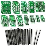
- 【Principle】: The transfer board is generally used for debugging and maintenance. Use it to import or export signals to connect test equipment or provide a signal source.
- 【Ideal for DIY Circuits】: You can use it to build many circuits. Ideal for school and college projects, beginners and advanced amateurs.
- 【Easy to Use】: The circuit board is neatly processed and easy to solder. They can also be soldered repeatedly. The pin header has good conductivity and can be directly inserted into the circuit board for easy use.
- 【High Quality】: All PCB prototype boards are double-sided and made of high quality FR4
- 【Various Models】: This kit has 12 types (51pcs) adapter boards, suitable for a variety of SMD chips.
The reported per-machine figures also vary: 8–15 FPS on an older i5 with integrated graphics, 15–25 FPS on an M1 MacBook Pro, and 18–28 FPS on an i7 with RTX 3050 Ti. Ayles does not specify all test conditions, so these numbers should not be treated as results from a controlled comparison.
What limits performance—and what it looks like
Ayles identifies KiCad’s pcbnew.Refresh() call as the bottleneck. He lists turning off the grid, ratsnest, antialiasing, and clearance outlines as ways to reduce overhead. The result remains a wireframe visualization rather than a textured game, and the project is not presented as smooth 60-FPS gameplay.
What’s actually slowing this PC down?
Pick the symptom - the matching free tool is one click away.
Rank #3

- 32 Boards In Five Sizes: Choose 4 × 6 cm, 3 × 7 cm, 5 × 7 cm, 2 × 8 cm or 7 × 9 cm boards for compact circuits, controller interfaces, classroom soldering exercises and larger point-to-point builds
- Double-Sided FR4 For Soldered Prototypes: Approximately 1.6 mm FR4 provides a rigid base for permanent electronics builds, while pre-tinned plated-through holes provide solderable connections accessible from both sides
- Standard 2.54 mm Grid Fits Common Through-Hole Parts: Lay out resistors, LEDs, DIP sockets, pin headers, terminal blocks, sensors and jumper wires on a 0.1 in pitch, then create each required connection with soldered leads, bridges or insulated wire
- From Breadboard Test To Permanent Build: Transfer a proven circuit into a compact soldered assembly for sensor nodes, controllers, alarms and STEM demonstrations; corner mounting holes help secure finished boards in enclosures or on panels
- Set Expectations Before Soldering: These are isolated-pad perfboards with no breadboard-style buses or stripboard traces, and the kit does not include components, wire, solder or tools; plan the layout and check continuity before applying power
The trade-off is clear: vector segments avoid the enormous object count implied by pixel-by-pixel drawing, but KiCad’s refresh behavior still constrains how quickly the rendered PCB view updates.
Independent reader supportYour contribution helps us test, update, and keep practical guides available for everyone.Can you try it?
Ayles’s project page describes building DOOM with the supplied script, trying the standalone renderer, installing a KiCad plugin, and launching it from PCB Editor’s External Plugins menu. Those are the author’s described steps, not independently verified installation instructions. The available project information here does not establish current repository availability, supported KiCad versions, or whether the setup works on a particular machine.
Rank #4

- Selection of Multi-Sized Proto Boards - 31 pieces double-sided prototype boards of 5 different size to meet your demands when designing your own Arduino kits, electronic experiments and DIY projects. (10 pieces 2*8cm, 10 pieces 3*7cm, 5 pieces 4*6cm, 5 pieces 5*7cm and 1 pieces 7*9cm PCB boards)
- Header Connector - 10 pieces 40 pin male header, 10 pieces 40 pin pitch right angle male headers, 10 pieces 40 pin female header; pitch: 2.54mm, single row and straight connector
- Screw Terminal Block - 8 pieces 5.08-301-2P and 5 pieces 5.08-301-3P ; pitch: 5.08mm, rated voltage: 300V, rated current: 16A
- Jumper caps - 30 pieces standard 2.54mm pin spacing circuit board jumper cap in 6 colors, 5 pieces per color
- Environmental and Elegant Packaging - Compact paper package take little footprint
KiDoom is best understood as a technical demonstration of an unusual rendering pipeline, not a practical PCB-design workflow. Its point is the visual conceit and the engineering needed to map game geometry onto PCB objects—not a new way to design boards or a reason to buy particular hardware.
Quick Recap
Best Value

- Professional Repair Solution:This high - quality rework pad is designed for mobile phone IC spot soldering and PCB pad repair. This pcb trace repair kit enables professional - level repairs without expensive equipment, making it ideal microsoldering kit for electronics repair shops and hobbyists.
- Superior Material & Construction:This pcb repair kit crafted from premium copper , this pcb pad repair kit offers excellent conductivity and heat resistance. This pcb trace pad repair kit ensures reliable connections even in challenging scenarios.
- Time & Cost - Efficient:Simply remove the protective layer and apply this replacement solder pad for quick, traceless repairs without circular marks, eliminating the need for flying wire techniques.
- Enhanced Stability & Flatness:Equipped with reinforced retaining pins to stay securely in place during soldering. Its exceptional flatness prevents virtual welding issues caused by uneven surfaces.
- Easy Application for BGA & PCB Repairs:Perfect for BGA pad restoration, PCB trace repair, and motherboard maintenance. It improves repair efficiency with seamless results, restoring circuit functionality without damaging surrounding components.
Product prices and availability are accurate as of the date/time indicated and are subject to change. Any price and availability information displayed on Amazon at the time of purchase will apply.

