
What’s actually slowing this PC down?
Pick the symptom - the matching free tool is one click away.
The Curtiss-Wright XF07-516 is a four-channel, 16-bit analog-input XMC card that samples each channel at 250MSPS and uses a user-programmable Xilinx Kintex-7 XC7K325T FPGA for processing on the card. It is designed for systems such as radar, SIGINT/ELINT, imaging, electronic warfare, and demanding test equipment—not as a general-purpose PC sound or data-acquisition card.
What the XF07-516 is
The XF07-516 Analog I/O XMC is an acquisition mezzanine: it fits into a compatible host system through the XMC (ANSI/VITA 42) form factor, rather than acting as a standalone instrument. Its defining combination is four simultaneous 16-bit inputs, each sampling at 250 million samples per second, and a programmable Kintex-7 FPGA on the card. Those specifications are identified in Curtiss-Wright’s product announcement and datasheet summary.
That combination suits applications that need to capture several analog signals and process them close to the point of conversion. The FPGA can run customer logic alongside acquisition; the vendor material also lists embedded digital downconverter (DDC) IP as an option.
XF07-516 specifications
| Feature | XF07-516 |
|---|---|
| Analog inputs | 4 channels |
| Resolution and sample rate | 16-bit; 250MSPS per channel |
| FPGA | User-programmable Xilinx Kintex-7 XC7K325T |
| Local memory | Two 128M × 16 DDR3 SDRAM banks; 512MB total |
| Host interface | XMC primary connector with x4/x8 PCIe path |
| Host operating systems | VxWorks and Linux support are stated in the product announcement |
| Cooling and operating temperature | Air-cooled and conduction-cooled variants; operation options stated down to -40°C to +85°C |
| Optional signal processing | Embedded DDC IP is listed in the datasheet summary |
The published material cited here does not specify the ADC analog bandwidth, PCIe generation, or a guaranteed sustained host-transfer rate. Those values should not be inferred from the 250MSPS sampling rate or the x4/x8 connector description.
Recommended Free Tools
#1 Best Overall

- 【PCILeech Friendly】64-bit Memory Access, PCIe TLP access, and PCILeech compatible. PCILeech utilizes the PCIe board with FPGA DMA to read and write to the target system memory. Note: our card does not come with any custom firmware.
- 【On/Off Switch】You can deactivate your card using the built-in on and off switch, eliminating the need to physically disconnect the device from your PC when you are not using the device.
- 【Layered Cooling】DMA card comes with an included heat sink ensuring optimal performance and longevity! This heatsink is further enhanced by a durable aluminum alloy cover. This layered cooling design helps prevent FPGA thermal throttling and overheating.
What 250MSPS means for data volume
At full resolution, four channels generate 16 billion bits per second before framing or any processing: 4 channels × 16 bits × 250 million samples per second. That is 2GB/s using decimal units, or about 1.86GiB/s. This is a calculation from the channel specifications, not a claim about measured or sustained transfer performance.
The listed 512MB of DDR3 provides local storage for acquisition and processing, but it does not by itself establish how long the card can record continuously or how quickly it can transfer data to a host. As a simple capacity estimate, 512MB would hold about 0.256 seconds of uncompressed, full-rate samples at 2GB/s, before accounting for memory organization, FPGA processing, protocol overhead, or other system behavior. Actual capture duration and throughput depend on the configured design and host.
Why put a programmable FPGA beside the inputs?
With a user-programmable XC7K325T on the mezzanine, designers can implement acquisition logic and customer algorithms near the converters instead of moving every raw sample to the host first. Depending on the design, FPGA processing could include filtering, detection, decimation, or channelization. These are examples of possible engineering uses, not performance claims or preloaded capabilities guaranteed by the product announcement.
Reducing or transforming data on the card may help a system fit within its host link or storage budget. The trade-off is that the required HDL, timing, memory use, and data path must be designed and validated for the application. The sources identify a user-programmable FPGA and customer-algorithm role, but do not establish a particular algorithm’s throughput or latency.
The Tool Desk
Outbyte Driver Updater FREEScan for outdated or missing drivers - takes under a minuteDriver Scan →Outbyte PC Repair FREERepair Windows errors before they cause bigger problemsFix Now →Rank #2

- Board, FPGA, development, EBAZ4205, ZYNQ
Does it fit a radar or SIGINT system?
Radar, imaging, SIGINT/ELINT, electronic warfare, and commercial or defense test equipment are among the stated application areas. Four simultaneous channels and FPGA processing make the card relevant when a design needs multi-input capture and custom real-time processing. Suitability for a specific system still depends on signal bandwidth, input range and conditioning, synchronization, clocking, data retention, and required interface performance.
Before selecting the card, confirm the full analog and system requirements with the vendor. In particular, the cited product information does not establish analog bandwidth, input voltage range, channel-to-channel synchronization details, or PCIe generation. Those omissions matter: sample rate alone does not tell you the highest input frequency the analog front end can capture accurately.
XF07-516 XMC versus a PXIe digitizer
An XMC card and a PXIe digitizer solve a similar acquisition problem but belong to different host ecosystems. The XF07-516 is a mezzanine intended for an XMC-capable host; the TSINGETECH PXIE301-136 is a four-channel PXIe alternative designed for a 3U PXIe system. The latter’s vendor information specifies PCIe Gen2 x8, 3.2GB/s DMA, 500MHz analog bandwidth, synchronization interfaces, and up to 4GB DDR3. These published PXIe figures are not equivalent measurements of the XF07-516.
| Consideration | Curtiss-Wright XF07-516 | TSINGETECH PXIE301-136 |
|---|---|---|
| Host format | XMC (ANSI/VITA 42) | 3U PXIe |
| Inputs | 4; 16-bit; 250MSPS per channel | 4; 16-bit; 250MSPS per channel |
| FPGA | Xilinx Kintex-7 XC7K325T | Xilinx Kintex-7 FPGA; exact model not stated in the cited product information |
| Local memory | 512MB DDR3 | Up to 4GB DDR3 |
| Host link | x4/x8 PCIe path; generation and sustained rate not stated in the cited product information | PCIe Gen2 x8; vendor-stated 3.2GB/s DMA |
| Analog bandwidth | Not stated in the cited product announcement or datasheet summary | 500MHz, according to TSINGETECH |
| Other stated system details | Air- or conduction-cooled variants; temperature options stated down to -40°C to +85°C | Synchronization interfaces are listed; cooling and operating temperature are not stated in the cited product information |
Choose based first on the host already available. An XMC design requires a compatible carrier or embedded host; a PXIe design requires a PXIe chassis and controller or compatible system. Then compare analog bandwidth, clocking and synchronization, environmental requirements, software and driver support, and the actual sustained data path. Published interface labels alone do not guarantee that an application will sustain its raw input rate.
Rank #3
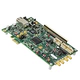
- EVALUATION BOARD: SmartFusion2 SoC FPGA Security PCIe Card featuring the M2S090 FPGA for development and testing purposes
- INTEGRATED SOLUTION: Combines FPGA capabilities with MCU/MPU System-on-Chip architecture for versatile application development
- DEVELOPMENT PLATFORM: Professional-grade board designed for security-focused PCIe applications and FPGA programming
- CONNECTIVITY: PCIe interface enables seamless integration with host systems for rapid prototyping and testing
- COMPATIBILITY: Purpose-built for SmartFusion2 FPGA development with comprehensive evaluation capabilities
Is an XC7K325T development board a substitute?
No. Puzhi documents an XC7K325T-2FFG900I FPGA development board and a “High Speed ADC-AD9643 Acquisition (250MSPS)” demonstration. That may be useful for prototyping or learning, but it is not a drop-in replacement for the XF07-516’s rugged XMC implementation, four-channel specification, cooling options, host integration, or software support.
A development board may require separate ADC hardware, FPGA design work, clocking, interfaces, and mechanical integration. Verify the board’s exact ADC configuration and capabilities rather than treating a 250MSPS demonstration as equivalent to the XF07-516.
Availability and purchase checks
Current production status, pricing, and sales availability are not established by the cited product materials. Contact Curtiss-Wright or an authorized reseller to confirm whether the XF07-516 is orderable and to obtain current configuration, support, and lifecycle information.
Quick Recap
- Confirm that the host accepts an XMC card and supports the required PCIe lane configuration.
- Ask for analog bandwidth, input characteristics, clocking and synchronization specifications, and sustained transfer details for the exact configuration.
- Verify which cooling and temperature variant is offered and whether its operating range suits the deployment.
- Confirm the available FPGA design tools, reference logic, DDC option, host drivers, and support for the intended VxWorks or Linux environment.
Product prices and availability are accurate as of the date/time indicated and are subject to change. Any price and availability information displayed on Amazon at the time of purchase will apply.

