
A hard macro is reusable intellectual property delivered as a largely fixed physical block: its layout geometry, pin locations, legal orientations and much of its timing behavior are defined for a target process. That makes it predictable and fast to integrate, but far less forgiving than synthesizable RTL. In a modern SoC, choosing, placing and connecting hard macros is an architectural decision that determines congestion, timing, power and die cost. Chiplets do not make this discipline obsolete; they extend it from the die to the package.
What a hard macro actually is
Physical IP, not just RTL
A soft IP block is normally supplied as RTL or another synthesizable description. A hard macro arrives with a physical implementation—layout geometry, cell arrangement, routing assumptions, abstract views, timing models and design-rule constraints—targeted to a particular process and set of interfaces. Integration still requires checks and sign-off, but the implementation team is not free to reshape the block as it would ordinary standard-cell logic.
Common examples
Hardening is especially valuable for dense or specialized functions. Typical examples include SRAM and other memories, analog and mixed-signal interfaces, processor subsystems, network-on-chip (NoC) fabrics, transceivers, DSP arrays and PCIe interfaces. Foundry memory compilers and vendor-supplied interface blocks are frequent sources of such macros.
Why teams use them
- Predictable capability: a validated physical block can provide a known interface, density and performance envelope.
- Reuse: the same implementation can be integrated into multiple products that use the same process and compatible constraints.
- Specialization: memories, analog circuits and high-speed I/O often cannot be replaced economically by generic standard cells.
- Risk concentration: verification and characterization are performed once for the block, then reused—provided the integration conditions remain within its model.
The trade-off is portability. A macro hardened for one process, voltage range or package assumption may need a new implementation, wrapper or timing model elsewhere.
#1 Best Overall

- Powerful Processor: Equipped with ESP32-S3R8 Xtensa 32-bit LX7 dual-core processor, up to 240MHz main frequency. Supports 2.4GHz Wi-Fi (802.11 b/g/n) and Bluetooth 5 (LE), with onboard antenna. Built-in 512KB of SRAM and 384KB ROM, with onboard 8MB PSRAM and an external 16MB Flash memory.
- Driver and Touch LCD: Onboard 1.83inch IPS Capacitive Touch Display, 240 × 284 resolution, 65K color. Built-in ST7789P display driver and CST816D capacitive touch chip, using SPI and I2C communication respectively, effectively saving the IO resources. Adopts Type-C port to improve user convenience and device compatibility.
- Supports Offline Speech recognition and AI Speech Interaction: Allows access to online large model platforms such as ChatGPT, DeepSeek, Doubao, etc. Onboard ES8311 audio codec chip and ES7210 echo cancellation circuit to meet daily audio application scenarios.
- Multifunctional Sensor: Onboard QMI8658 6-axis IMU (3-axis accelerometer and 3-axis gyroscope) for detecting motion gestures, counting steps, etc; PCF85063 RTC chip connected to the battry via the AXP2101 for uninterrupted power supply; Onboard PWR and BOOT programmable buttons for easy custom function development.
- Rich Peripheral Interface: Reserved 1 × I2C, 1 × UART and 1 × USB pads for external device connection and debugging, enabling flexible peripheral configuration. Onboard TF card slot for extended storage and fast data transfer, suitable for applications such as data recording and media playback, simplifying circuit design.
Why macro placement is an architectural decision
Fixed geometry constrains the floorplan
A macro’s width, height, aspect ratio, pin locations and legal orientations are largely predetermined. Some blocks can be mirrored or rotated only in specific ways; others must occupy designated sites or keep-out regions. Power straps, clock structures and neighboring standard-cell rows must be planned around those restrictions.
Placement changes the whole chip
Distance and orientation determine wirelength, routing layers, pin access, buffering and clock skew. A locally excellent macro can therefore produce a poor chip if it blocks channels, isolates logic that communicates frequently or forces long detours around a cluster. The relevant objective is not merely the macro’s area; it is the quality of the complete floorplan.
| Physical choice | System-level consequence |
|---|---|
| Macro location | Changes interconnect length, congestion, timing margin and power consumed by long nets. |
| Orientation or mirroring | Changes which sides expose pins and how power, clock and data routes enter the block. |
| Aspect ratio and spacing | Changes channel capacity, standard-cell utilization and the amount of unused or inaccessible silicon. |
| Pin access and routing layers | Changes whether signals can escape without detours, extra vias or local congestion. |
| Site and keep-out rules | Restrict legal placements and may force other logic, clocks or power structures to move. |
Why more macros can enlarge the die
Each additional fixed block removes freedom from the placer. Macro-heavy designs can leave unusable slivers, blocked routing channels and low-utilization regions even when an abstract RTL estimate appears compact. If the architecture and floorplan are optimized separately, a resource-sharing decision that saves logical area can concentrate traffic in one corridor and require a larger die to close timing and routing.
Rank #2

- 2pcs NRF51822 sensor
EE Times reported this concern in its August 20, 2004 article, quoting a survey of more than 175 design teams at that year’s Design Automation Conference. Its two stated priorities were access to a broad set of flexible hard-macro implementations—especially memory compilers—and the ability to place those macros so congestion is minimized and utilization maximized. The article’s economic illustration was historical: an EE Times analysis of a 0.13 µm foundry-pricing example estimated that a 10% reduction on a three-million-unit IC could increase margin by more than $6 million. That figure is not a current industry benchmark.
What’s actually slowing this PC down?
Pick the symptom - the matching free tool is one click away.
How hard macros change the design flow
The search space grows rapidly
With many macros, implementation must explore combinations of location, orientation, flipping, spacing, aspect ratio, pin access and the standard-cell logic surrounding each block. The interactions are combinatorial: moving one memory can open a channel for one path while closing the only practical route for another.
Architecture and physical planning must meet earlier
High-level models that report only logical area or operation count can miss the cost of concentrated wires and restricted sites. Macro-aware exploration should therefore test physical consequences while architectural choices are still changeable.
Rank #3
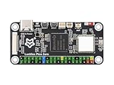
- Powerful Processing Core: Equipped with a single-core ARM Cortex-A7 32-bit processor, featuring integrated NEON and FPU for efficient computation and optimized performance.
- Advanced NPU for High Precision: Built-in Rockchip self-developed 4th generation NPU, supporting int4, int8, and int16 hybrid quantization, delivering 1 TOPS of computing power for enhanced AI capabilities.
- High-Quality Imaging: Features Rockchip's third-generation ISP3.2 with 8MP support and advanced image enhancement algorithms, including HDR, WDR, and multi-level noise reduction for superior image quality.
- Efficient Encoding Performance: Supports intelligent encoding mode and adaptive stream saving, reducing bit rates by over 50% compared to conventional CBR mode while maintaining high-definition image quality with smaller file sizes.
- Robust Memory Capacity: Built-in 16-bit 256MB DRAM DDR3L, offering the necessary memory bandwidth to handle demanding applications and ensure seamless performance.
- Inventory the hard IP: record dimensions, legal orientations, voltage domains, timing models, power data, keep-outs, preferred layers and interface directions.
- Map communication: identify bandwidth, latency and synchronization requirements between each macro and the surrounding compute, memory and I/O logic.
- Create alternative floorplans: vary clusters, channels, orientations and macro-to-logic relationships rather than committing to a single sketch.
- Estimate implementation effects: evaluate congestion, utilization, wirelength, timing, power and clock feasibility for each alternative.
- Refine the architecture: change partitioning, pipeline boundaries, data movement or sharing when the physical results expose a bottleneck.
- Re-run sign-off-oriented analysis: confirm that the selected plan remains valid under extracted parasitics, process corners, power integrity and thermal constraints.
This loop does not eliminate detailed place-and-route work; it prevents an apparently efficient architecture from becoming an expensive physical exception late in the schedule.
Timing and routing behavior of hardened blocks
Dedicated resources are not ordinary flip-flop fabric
AMD’s 2024.2 design methodology for Versal devices (released December 18, 2024) warns that dedicated blocks such as DSPs and block RAM can have higher setup or hold requirements, higher clock-to-output values on some pins, greater routing delay and more clock-skew variation than ordinary flip-flop paths. Their restricted sites make placement harder and can reduce quality of results.
Quick wins for a faster PC:
Repair Windows errors before they cause bigger problemsFix Now →Scan for outdated or missing drivers - takes under a minuteDriver Scan →Clear out junk files and repair common Windows errorsFree Scan →A concrete block-RAM example
| Configuration | Clock-to-output value reported by AMD UG949 (2024) |
|---|---|
| Block RAM without an output register | About 1.5 ns |
| Block RAM with an output register | About 0.4 ns |
These are the guide’s example values, not universal numbers for every device, speed grade or operating condition. The register changes the latency and interface behavior, so it must be evaluated with the surrounding pipeline rather than treated as a free timing fix.
Rank #4

- ESP32-P4-NANO development board based on ESP32-P4 chip, high-performance MCU with RISC-V 32-bit dual-core and single-core processors. 128 KB HP ROM, 16 KB LP ROM, 768 KB HP L2MEM, 32 KB LP Static RAM, 8 KB TCM. 32MB PSRAM in the chip's package, with onboard 16MB Nor Flash
- Onboard ESP32-C6-MINI module to extend 2.4GHz Wi-Fi 6 and Bluetooth 5/BLE for ESP32-P4, using SDIO interface protocol for communication, stable connection and efficient transmission. Reserved PoE Module header, more flexible for Power Supply
- Commonly used peripherals such as MIPI-CSI, MIPI-DSI, USB 2.0 OTG, Ethernet, SDIO 3.0 TF card slot, microphone, speaker header and RTC battery header, etc. Adtaping 2*2*13 GPIO headers with 28 x programmable GPIOs
- Powerful image and voice processing capability. Provides image and voice processing interfaces including JPEG Codec, Pixel Processing Accelerator, Image Signal Processor, H264 encoder
- Security features: Secure Boot, Flash Encryption, cryptographic accelerators, and TRNG. Additionally, hardware access protection mechanisms help to enable Access Permission Management and Privilege Separation
Typical responses when distance hurts timing
- Pipeline the interface or add an output register where the protocol permits it.
- Reduce logic depth between the macro and its consumers.
- Replicate a logic cone when one distant block would otherwise drive multiple regions.
- Use the device’s dedicated timing-optimization features and legal placement resources.
- Reconsider macro clustering, data locality or the partition itself before applying increasingly aggressive buffering.
Hard macros remain central in current SoCs
What the Versal methodology illustrates
AMD’s Versal 2024.2 guide says every Versal adaptive SoC design includes at least part of the Control, Interface and Processing System (CIPS). CIPS contains the platform-management controller, processor subsystems and a cache-coherent PCIe module. The same methodology describes the NoC as a high-bandwidth, hardened interconnect and the only route to Versal’s hardened memory controllers.
The example matters beyond one product family: modern SoCs commonly combine programmable logic with processor, memory, I/O and interconnect functions that are delivered as hardened resources. Those resources make system planning more deterministic, but they also make placement, interfaces and traffic patterns part of the architecture.
Independent reader supportYour contribution helps us test, update, and keep practical guides available for everyone.Do chiplets make hard macros obsolete?
The hierarchy has gained another level
The ACM survey Chiplet Design Automation: Methodologies, Advances, and Directions describes a move from an IP–chip hierarchy to an IP–chiplet–chip hierarchy. A reusable block may now be integrated inside a die, delivered as a complete chiplet, or combined with other dies in a package. In each case, its interface, physical assumptions and verification evidence still have to compose with the rest of the system.
Best Value

- with pre-soldered header Raspberry Pi Pico. RP2040 microcontroller chip designed by Raspberry Pi in the United Kingdom
- Dual-core Arm Cortex M0+ processor, flexible clock running up to 133 MHz. 264KB of SRAM, and 2MB of on-board Flash memory.
- Castellated module allows soldering direct to carrier boards. USB 1.1 with device and host support. Low-power sleep and dormant modes. Drag-and-drop programming using mass storage over USB. 26 × multi-function GPIO pins.
- 2 × SPI, 2 × I2C, 2 × UART, 3 × 12-bit ADC, 16 × controllable PWM channels.Accurate clock and timer on-chip.Temperature sensor.
- Accelerated floating-point libraries on-chip.8 × Programmable I/O (PIO) state machines for custom peripheral support
What moves from die planning to package planning
| Decision | On-die macro question | Chiplet-level question |
|---|---|---|
| Partition boundary | Which logic and memories share a die? | Which functions justify separate dies or process nodes? |
| Interconnect | Can pins escape with acceptable wirelength, congestion and timing? | Can die-to-die links provide the required bandwidth and latency? |
| Cost | Will macro area and low utilization enlarge the die? | Will extra dies, package routing and assembly cost outweigh node specialization? |
| Parasitics | What routing and clock parasitics result inside the die? | What package and inter-chiplet interconnect parasitics result at the boundary? |
| Verification | Do abstracts, timing models and physical views match sign-off? | Do die interfaces, protocols, power delivery and package models match system sign-off? |
Chiplets therefore extend macro-aware planning rather than replace it. The optimization target now includes process-node specialization, package-level cost, inter-chiplet bandwidth and interconnect parasitics in addition to on-die placement and routing.
What automation can realistically improve
Macro placement is an optimization problem
Automation is useful when it evaluates architectural alternatives instead of merely polishing one fixed floorplan. It must understand legal orientations, pin access, blockages, timing-critical nets, power domains and the standard-cell regions that remain after macros are placed.
Reported IncreMacro results
The ISPD 2024 IncreMacro paper reports the following improvements over its baselines on its test cases:
| Metric | Reported improvement |
|---|---|
| Routed wirelength | 6.5% and 16.8% in the paper’s two baseline comparisons |
| Worst negative slack | 59.9% and 99.6% |
| Total negative slack | 63.9% and 99.9% |
| Total power | 3.3% and 4.9% |
These percentages are benchmark results for that paper’s experimental cases. They are not guarantees for a production design, a particular process or every macro-placement tool.
The Tool Desk
Outbyte Driver Updater FREEFix the driver behind crashes, sound loss and screen glitchesFind Drivers →Outbyte PC Repair FREERepair Windows errors before they cause bigger problemsFix Now →How to compare hard-macro strategies and tools
| Evaluation axis | Questions to ask |
|---|---|
| Process portability and reuse | Can the block move between process variants, voltage domains or products, and what must be re-hardened? |
| Area, utilization and die cost | How much whitespace, channel blockage and aspect-ratio compromise does the macro set create? |
| Timing and congestion | Does the flow optimize critical paths and routing together, including pin access and extracted parasitics? |
| Power and thermal behavior | Are switching, leakage, power delivery and thermal concentration evaluated at the intended operating conditions? |
| Physical flexibility | Which orientations, aspect ratios, pin sides, voltage regions and placement sites are legal? |
| Verification and model quality | Are abstracts, timing, power, noise and physical-verification views complete and consistent? |
| Cross-level optimization | Can the method co-optimize architecture, macro placement, die partitioning and chiplet/package choices? |
The enduring design lesson
Hard macros deliver capabilities that generic logic cannot efficiently reproduce, but they turn physical implementation into part of the system specification. The successful approach is to treat macro selection, interfaces, placement and traffic as one problem: explore alternatives early, measure whole-chip consequences, and carry the same discipline across chiplet and package boundaries. That is why the 2004 prediction still resonates in current SoC work—not because every block should be hardened, but because reusable physical blocks increasingly determine what the rest of the chip can achieve.
Quick Recap
Product prices and availability are accurate as of the date/time indicated and are subject to change. Any price and availability information displayed on Amazon at the time of purchase will apply.

