
Quick wins for a faster PC:
Fix the driver behind crashes, sound loss and screen glitchesFind Drivers →Clear out junk files and repair common Windows errorsFree Scan →Scan for outdated or missing drivers - takes under a minuteDriver Scan →Vertical GaN is a power-device architecture in which current flows through the thickness of the device rather than along its surface. It is designed to use gallium nitride’s high breakdown field and switching speed at higher voltages, but it remains an emerging technology with demanding substrate, fabrication, and reliability challenges.
What is vertical GaN?
Vertical GaN is a gallium nitride power device built so that current travels down through the device structure. A thick, lightly doped drift layer blocks voltage when the device is off and conducts current when it is on. The highest electric fields are designed to occur inside the structure, often near buried junctions, rather than mainly at the surface.

In a January 19, 2022 EE Times PowerUP episode, Sandia National Laboratories’ Robert Kaplar described vertical GaN devices as analogues of discrete silicon or silicon-carbide power devices. That analogy helps distinguish their construction from the surface-oriented GaN transistors commonly used in switching converters.
How does vertical GaN differ from lateral GaN?
Lateral GaN high-electron-mobility transistors (HEMTs) use a heterostructure that creates a two-dimensional electron gas (2DEG) near the surface. Current flows sideways through this channel. Vertical devices instead conduct through the device thickness, typically using a GaN drift layer and a native GaN substrate.
#1 Best Overall
| Design consideration | Lateral GaN | Vertical GaN |
|---|---|---|
| Current path | Along a surface channel in a heterostructure, using a 2DEG near the surface (Kaplar, EE Times, Jan. 19, 2022). | Through the device thickness, through a drift layer and typically a GaN substrate (Kaplar, EE Times, Jan. 19, 2022). |
| Voltage scaling | As voltage rises, gate-to-drain spacing must increase, taking more die area. An EE Times APEC discussion in 2022 described lateral devices then available from 100 V to 650 V and mentioned a 900 V product; those are dated examples, not a current market census. | The 2022 APEC discussion said voltage could be increased with comparatively little change in lateral wafer area, apart from edge termination. It did not give a vertical-device voltage range. |
| Typical design emphasis | The episode characterized lateral GaN as tending toward lower-voltage, lower-power applications with very high switching frequency (Kaplar, EE Times, Jan. 19, 2022). | Intended to extend GaN power-device use toward higher voltage and current handling; the episode did not establish a universal voltage or current rating. |
| Substrate and fabrication | Uses a surface heterostructure; the episode does not state a comparable substrate or manufacturing-cost specification. | Typically uses a native GaN substrate and requires high-quality bulk material and thick drift-layer epitaxy (Kaplar, EE Times, Jan. 19, 2022). |
The core trade-off is architectural, not a blanket claim that one device is better. Vertical construction offers a way to scale voltage without continually lengthening a surface channel, while lateral GaN has been used where fast switching and compact surface devices suit the application. Actual performance depends on the device and its design; the episode does not supply a controlled, product-to-product comparison of on-resistance, thermal behavior, reliability, or cost.
Why use GaN on GaN substrates?
A native GaN substrate gives the vertical structure a path to combine GaN’s material properties with a through-thickness current path. The approach aims to exploit GaN’s high breakdown field, high switching speed, and power-density potential in devices intended for voltages where lateral scaling can become difficult.
Rank #2
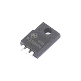
- 2 Pcs Gallium Nitride Transistor (GaN HEMT) RC65D600A RC65D600A TO-220F
The substrate is not simply a packaging choice: the vertical device depends on a high-quality bulk GaN base and a carefully grown drift layer above it. A thick drift region must block voltage while remaining lightly doped enough for that purpose. Defects that compensate or disrupt the intended doping can undermine the layer’s electrical behavior, making material quality and epitaxy central to whether the architecture can be manufactured consistently.
Can vertical GaN replace silicon carbide at high voltage?
Vertical GaN is a potential alternative in some high-voltage power-conversion applications, not an established general replacement for silicon carbide (SiC). The EE Times episode presents vertical GaN as promising, but the information it provides does not establish a universal voltage crossover, equivalent commercial product set, or cost advantage over SiC.
Rank #3

- Transistor type: MOSFET
- Transistor polarity: N-Channel
- Drain current (Id Max): 110A
- Voltage Vds Max: 55V
- Power(Max): 200W
A fair comparison has to account for more than breakdown voltage. It also depends on on-resistance, current handling, switching frequency, thermal path, edge termination, reliability, substrate availability, manufacturing yield, and cost. The cited coverage describes vertical GaN as earlier-stage than mature lateral GaN and SiC offerings, so suitability needs to be judged against a particular application and an actual device’s specifications.
What engineering challenges remain?
- Bulk substrates and epitaxy: High-quality GaN substrates and scalable growth of the device layers are necessary for repeatable vertical structures.
- Drift-layer control: Growing a thick, lightly doped layer while controlling compensating defects is difficult and directly affects voltage blocking and resistance.
- Field management: Edge termination must control electric fields at the perimeter of the device, where breakdown can otherwise occur before the interior structure reaches its design limit.
- Gate and thermal design: Gate dielectrics, heat removal, and the device’s thermal path require robust solutions for practical power operation.
- Reliability and manufacturing: The technology must move from demonstrations to repeatable, economical production, with processing and long-term reliability validated at scale.
Where might vertical GaN be used?
The application areas discussed in EE Times coverage are systems that need high-power conversion, potentially with benefits from higher operating voltage or compact, efficient power electronics. These are directions for development, not proof that vertical GaN is already deployed broadly in each sector.
Rank #4
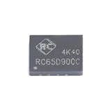
- 5 Pcs Gallium Nitride Transistor (GaN HEMT) RC65D900C GaN Field Effect Transistor DFN-8 (5x6)
- Automotive: Electric-vehicle drivetrains and other high-power conversion stages.
- Aviation, rail, and marine: Medium-voltage electrification, where higher system voltage can help reduce cable mass.
- Energy and grid infrastructure: Renewable-energy integration, storage, grid resiliency, solid-state substations, transformers, and specialized arrestor-related work.
- Data centers: Emerging positioning for power infrastructure where efficiency and power density matter; this application was highlighted in later engineering coverage.
What do the early commercial demonstrations show?
EE Times coverage named companies pursuing vertical-conduction or vertical-GaN devices and reported two NexGen demonstration figures in 2022. These examples indicate development activity; they do not by themselves establish broad commercial availability, production scale, or performance relative to competing products.
| Company or demonstration | What the coverage reported |
|---|---|
| Odyssey Semiconductor | Discussed in the episode in connection with high-voltage vertical-conduction devices; no specific rating is stated in the episode summary (EE Times, Jan. 19, 2022). |
| NexGen power supply | A 240 W power-supply demonstration was reported in the 2022 EE Times APEC discussion. |
| NexGen isolated LED driver | A 20 W isolated LED-driver demonstration was reported in the 2022 EE Times APEC discussion. |
The wattage figures describe the reported demonstrations, not a general rating for vertical GaN devices or evidence of current product availability.
The Tool Desk
Outbyte PC Repair FREERepair Windows errors before they cause bigger problemsFix Now →Outbyte Driver Updater FREEScan for outdated or missing drivers - takes under a minuteDriver Scan →Quick Recap
Best Value

- 5 Pcs Gallium Nitride Transistor (GaN HEMT) MX1020W Gallium Nitride High Speed Driver CSP-6
Product prices and availability are accurate as of the date/time indicated and are subject to change. Any price and availability information displayed on Amazon at the time of purchase will apply.

