
When a TC4420 simulation fails in LTspice, the usual cause is model integration or wiring—not an inherent inability to simulate the driver. Check the model’s exact .SUBCKT declaration, symbol pin order, duplicated supply and ground pins, and the input/output references before debugging the MOSFET power stage.
Identify the failure before changing the circuit
| Symptom | Most likely area |
|---|---|
| “Unknown subcircuit” or missing model | Missing .include, wrong file path, or wrong subcircuit name |
| “Too few nodes” | Symbol pin count does not match the model declaration |
| Flat output | Supply, ground, input connection, or pin-order error |
| Inverted output | TC4429 selected accidentally, or an inverted symbol/model |
| MOSFET does not switch | Incorrect gate-to-source reference, MOSFET model, or power-stage wiring |
| “Singular matrix” | Floating node, missing ground, or ideal source/capacitor combination |
| “Timestep too small” | Ideal transitions, severe stiffness, unrealistic parasitics, or floating nodes |
Confirm that the device and electrical assumptions are correct
The TC4420 is a non-inverting, single-output, low-side MOSFET gate driver. The TC4429 is its inverting companion, so importing a TC4429 model is an easy way to obtain apparently reversed logic. Microchip specifies a 4.5 V to 18 V supply range and a logic-high input requirement of 2.4 V to VDD. A 3.3 V or 5 V pulse is normally suitable when VDD is in range; a pulse below 2.4 V may not qualify as high.
Microchip lists a 6 A peak CMOS push-pull output. That is a peak-drive specification, not a continuous output-current rating. Datasheet timing figures—approximately 55 ns propagation delay and 25 ns rise/fall time with the stated test load—depend on supply, capacitance, temperature, and other test conditions; they are not promises that every LTspice macromodel will produce those exact values. See the TC4420 product page and DS21419D datasheet.
Check the standard 8-pin package
| Physical pin | Function |
|---|---|
| 1 | VDD |
| 2 | INPUT |
| 3 | NC |
| 4 | GND |
| 5 | GND |
| 6 | OUTPUT |
| 7 | OUTPUT |
| 8 | VDD |
Microchip specifies that the duplicate VDD, GND, and OUTPUT pins be connected. This physical package order is not proof that a downloaded subcircuit uses the same order. The model’s own declaration is authoritative. Five-pin and eight-pin versions must not be mixed.
#1 Best Overall
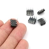
- Package / Case: PDIP-8
- Number of Drivers: 1 Driver
- Operating Supply Voltage: 4.5 V to 18 V
- Pd - Power Dissipation: 730 mW
- Number of Outputs: 1
Make sure LTspice has the right model
LTspice does not include every manufacturer model. Microchip provides TC4420/TC4429 SPICE resources on the product page. It also lists a TC4420 analog-simulation package for MPLAB Mindi, dated August 26, 2025, at its simulation-library page. A Mindi package is not automatically an LTspice-ready library.
Open the downloaded file in a text editor and locate a line such as:
Rank #2

- Logic Input Will Withstand Negative Swing Up to 5V.
- High Peak Output Current 6A
- Wide Operating Range 4.5V to18V.
- Low Output impedance
- NOTE:Exposure to absolute maximum rating conditions for extended periods may affect device reliability. We do not provide technical support, please familiarize yourself with the parameters and performance of the purchased products in advance. Sincerely apologize for you.
.SUBCKT TC4420 ...Record the exact subcircuit name, external-pin count, pin order, and any nested .include files. Do not assume that the filename, symbol value, and subcircuit name match. Encrypted sections, PSpice-specific syntax, unsupported functions, or missing dependencies can also prevent import.
Import a subcircuit correctly
- Save the model file in the same directory as the schematic, or use an explicit path.
- Place a SPICE directive on the schematic, for example
.include TC4420.lib. - Use a symbol with the same number of external pins as the
.SUBCKTdeclaration. Edit or create a custom symbol if necessary. - Set the symbol prefix to
X; subcircuit instances require anXelement prefix. - Set the symbol’s model or value field to the exact name after
.SUBCKT. - Open View → Spice Netlist and verify the include line, an
X...instance, the intended subcircuit name, and the intended node order. Analog Devices describes this import and netlist-checking workflow in its third-party model guide.
A conceptual physical-order instance might look like:
Recommended Free Tools
Rank #3
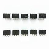
- Item Condition: Brand New
- Quantity: 10 Pcs TC4420 TC4420C TC4420CP TC4420CPA DIP-8 High-Speed MOSFET Drivers
- Actual item as shown in photos
- Random send the part number
- NOTE: Kindly compare your original item with the photos provided for the listing to make sure that you are purchasing the correct part. we don't provide technical assistance please make sure you are familiar with the product before purchasing. apologize in advance
XU1 VDD IN NC GND GND OUT OUT VDD TC4420This is only an example. Replace both the name and node order with the values in your downloaded .SUBCKT line. A symbol whose graphic pin numbers look correct can still netlist in a different order.
Test the driver without a MOSFET
First isolate the driver. Use a valid supply, a clean logic pulse, a common ground, and a modest capacitive load:
Rank #4

- 10pcs TC4420CPA TC4420C TC4420 IC MOSFET DRIVER 6A HS DIP8. IC
VDD VDD 0 12
VIN IN 0 PULSE(0 5 0 2n 2n 500n 1u)
CLOAD OUT 0 2.5n
RPROBE OUT OUT_MEAS 1m
.tran 0 5u 0 0.5n
Instantiate the model according to its actual pin declaration. The 2.5 nF load corresponds to a common datasheet timing test condition; it is not a universal load recommendation. The 0.5 ns maximum timestep is a diagnostic choice for seeing nanosecond transitions, not a TC4420 requirement.
Probe V(IN) and V(OUT). A correctly mapped TC4420 should be non-inverting: low input produces a low output and high input produces an output approaching the driver supply, subject to the model and load. If the input is absent, below the logic threshold, connected to the wrong subcircuit pin, or displayed over too long a time span, the output can appear dead even when the model is functioning.
Best Value

- 10pcs/lot TC4420EPA TC4420CPA TC4420 DIP-8
Check input-edge quality
Use a clean pulse before testing a slow ramp, op-amp output, or heavily loaded logic signal. Microchip warns that slow input edges can cause double-pulsing. Confirm the pulse amplitude, rise and fall times, width, period, ground reference, and displayed time window.
Independent reader supportYour contribution helps us test, update, and keep practical guides available for everyone.Verify output and MOSFET measurements
Measure the driver output relative to its ground, not an unrelated reference. In a floating or named-reference circuit, use V(OUT)-V(GND). After adding the MOSFET, inspect V(G,S), not only the gate node. A correct low-side driver output can fail to switch a MOSFET if the source moves, the gate-source reference is wrong, the device requires a different gate voltage, or its gate-charge and capacitance model differs from expectations.
Use staged substitution:
- Replace the TC4420 with an ideal or behavioral voltage source.
- Confirm that the MOSFET and power stage switch correctly.
- Restore the TC4420 model.
- If failure appears only after restoration, return to the include, pin mapping, and compatibility checks.
- If both versions fail, investigate the MOSFET, topology, supply, ground, and gate-source reference.
Resolve common LTspice errors
Unknown subcircuit
- Confirm the schematic contains the correct
.includedirective. - Check the file path and spelling.
- Match the symbol value exactly to the
.SUBCKTname. - Include every nested library file required by the model.
Too few nodes
- Compare symbol pin count with the declaration.
- Check for hidden or unconnected pins.
- Ensure a model for the correct package is selected.
Singular matrix
- Add the circuit ground and inspect for floating nodes.
- Check every model pin connection.
- Provide a DC path around ideal capacitors and sources where appropriate.
- Reduce the circuit to the driver-only test.
Timestep too small
- Give pulse sources finite rise and fall times.
- Add realistic series resistance to ideal inductors, capacitors, and gate connections.
- Remove floating nodes and extreme ideal current spikes.
- Reduce circuit complexity before lowering the maximum timestep.
- Use startup or initial-condition options cautiously and document them.
Supply bypassing and hardware realism
For hardware-oriented simulations, place a local ceramic bypass capacitor from VDD to ground; Microchip suggests a minimum of 1 µF. Short, low-inductance supply and ground paths matter because the ground pins carry bias and high peak gate-discharge currents. The bypass capacitor may not be required for a simplified macromodel to produce an output, so distinguish a simulation-node requirement from a real-board requirement. Microchip’s layout guidance is in AN798.
Also remember that a macromodel may omit package parasitics, detailed supply-current transients, thermal effects, or simulator-specific behavior. If the model uses incompatible syntax, is encrypted, or was intended for Mindi, use the intended environment or substitute a clearly labeled behavioral driver. An ideal source is useful for topology and PWM debugging, but it does not reproduce propagation delay, output resistance, current limiting, or nonlinear internal behavior unless you add those deliberately.
Diagnostic order that minimizes wasted time
- Confirm the downloaded file and any dependencies exist.
- Read the exact
.SUBCKTname, pin count, and order. - Set the symbol prefix to
Xand inspect the generated netlist. - Connect VDD, both grounds, duplicated outputs, and the input according to the model.
- Use VDD between 4.5 V and 18 V and a clean pulse above the 2.4 V high-level specification.
- Run the capacitive-load driver-only test.
- Probe output relative to driver ground.
- Add the MOSFET and inspect gate-to-source voltage.
- Replace the model with an ideal source to isolate any remaining power-stage fault.
The Bottom Line
Fix the model reference and pin order first, then prove the TC4420 with a clean pulse and capacitive load. Only after its output is correct should you debug MOSFET gate-to-source voltage, topology, and hardware parasitics.
Quick Recap
Product prices and availability are accurate as of the date/time indicated and are subject to change. Any price and availability information displayed on Amazon at the time of purchase will apply.

