
Yes. An op-amp can drive a MOSFET gate directly when it is regulating a slow or moderate-speed linear circuit, such as a current sink or electronic load. For fast, repetitive switching—especially PWM, converters, and motor drives—a dedicated gate-driver IC is usually the better choice. The key distinction is that an op-amp closes a precision feedback loop; a gate driver supplies the large transient current needed to switch a capacitive gate quickly.
What an op-amp driving a MOSFET means
The op-amp compares a reference with a sensed voltage and adjusts the MOSFET’s gate-to-source voltage until the feedback signal approaches the reference. In a linear circuit, the MOSFET may sit partly on rather than switching fully on and off.
Low-side current-sink example
                 Load
Supply ----------//------ Drain
                              N-channel MOSFET
Reference ---------------- (+) op-amp
Sense resistor voltage ---- (-) op-amp
Op-amp output ---- RG ---- Gate
Source -------------------- Sense resistor ---- Ground
                         RGS from gate to source
The op-amp drives the gate until the sense voltage is approximately the reference voltage. For this low-side arrangement, the nominal load current is:
I ≈ VREF / RSENSE
For example, with a 1.0 V reference and a 0.5 Ω sense resistor, the target current is about 2 A. The resistor dissipates I²R = 2 W at that current, so select a suitably rated part with thermal margin. If the MOSFET has 10 V across it at 2 A, it dissipates 20 W. Accurate current regulation does not make that heat disappear.
Free tools Windows power users keep installed
One-click scans. No signup required.
#1 Best Overall
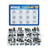
- BOJACK high quality 12 Values 120 Pcs IC Assortment Kit
- Packed Sorted accordingly in A Plastic Storage Case
- Huge IC Assortment contains: LM324N, LM339N, ULN2003AN, ULN2803APG, LM358P, LM386, LM393, NE5532P, NE555P, UA741CN , JRC4558D, PC817
- Including 12 pcs DIP8 socket, 4 pcs DIP14 socket, 2 pcs DIP16 socket, 2 pcs DIP18 socket
- Contains various usefull IC types such as: Photocouplers,Timers,Osciallators, Dual Opamps, Quad Opamps, Comperators, Audio Amplifiers, Echo Processors, Current Mode Controllers, Darlington Arrays, Voltage Charge Pump
When direct op-amp drive is appropriate
Direct drive is useful when the MOSFET is a controlled element in a feedback loop and the gate does not need fast, high-current transitions. Typical applications include constant-current sinks, electronic loads, linear LED regulators, pass elements, battery chargers, and slow actuators.
The gate draws very little steady-state DC current, but it is not a current-free load: the op-amp must source or sink transient current when changing the gate voltage. Whether direct drive works depends on the MOSFET’s gate charge, the required response time, the op-amp’s output swing and current capability, and loop stability.
When a dedicated gate driver is better
Use a gate-driver IC for high-frequency PWM, power converters, half-bridges, motor inverters, large-gate-charge MOSFETs, or designs that need short switching transitions. A driver is designed to deliver and remove substantial transient gate current; an ordinary op-amp generally is not.
For switching, a useful first estimate is IAVG ≈ QG × f, where QG is total gate charge and f is switching frequency. Approximate gate-drive power is P ≈ QG × VDRIVE × f. TI explains these relationships and the role of Miller charge in its UCC27322-Q1 datasheet. Gate charge varies with operating conditions, so use the MOSFET datasheet’s specified conditions when estimating.
For example, a 50 nC gate changed in 1 μs requires about 50 mA average during that transition. At 10 kHz and 10 V drive, the simplified average gate-charge power estimate is 5 mW. Low average power does not mean low peak-current demand: the op-amp output stage still has to supply the transition current repeatedly. Microchip’s AN799 driver-matching guidance discusses matching driver capability and MOSFET gate charge to the required switching time.
Rank #2

- IC Assortment contains: LM324, LM358, LM386, LM393, UA741, NE5532,NE555,PC817,ULN2003,ULN2803
- Including 10 pcs DIP4 socket, 60 pcs DIP8 socket, 5 pcs DIP14 socket, 5 pcs DIP16 socket,5 pcs DIP18 socket
- We have chosen a variety of useful IC types for daily assembly, such as: precision timers, dual operational amplifiers, audio amplifiers, Darlington arrays, quad operational amplifiers, etc.
- Anti-static plastic box, store commonly used IC kits according to label instructions
- ULN2003,ULN2803:ULN2003, ULN2803: 10 pcs Darlington array
| Requirement | Op-amp directly driving the MOSFET | Dedicated gate driver |
|---|---|---|
| Precision analog current regulation | Good fit as the feedback amplifier | Does not replace the feedback control loop |
| Slow linear control | Often appropriate if swing, current, and stability are adequate | Usually unnecessary by itself |
| Fast PWM or power switching | Often limited by output current and capacitive-load stability | Designed for fast gate charging and discharging |
| High-side N-channel MOSFET | Ground-referenced output is generally insufficient | Use a suitable high-side drive arrangement |
| MOSFET linear-mode heating | Must be checked independently | A driver does not solve MOSFET dissipation |
Choose the MOSFET for its real operating conditions
- Gate voltage: Check the datasheet’s
RDS(on)test voltage against the gate voltage the op-amp can actually provide.VGS(th)is the point where a small specified current begins to flow; it does not guarantee low on-resistance or full load operation. - Absolute maximum gate voltage: Keep
VGSwithin its limit, including transients. The gate voltage is measured relative to the source, which may not be at ground. - Switching demand: For transitions, use total gate charge
QGand Miller chargeQGD, not input capacitance alone. Gate capacitance is nonlinear, and drain-voltage movement contributes to the Miller plateau. - Voltage, current, and thermal limits: Check
VDS, current, package dissipation, thermal resistance, and body-diode behavior against worst-case conditions. - Linear operation: Check the MOSFET’s DC safe operating area (SOA). A device optimized for low switching losses or low
RDS(on)is not automatically suitable as a continuously dissipating pass element.
In linear operation, calculate PMOSFET = VDS × ID for the worst-case voltage and current combination. Then assess junction temperature using the applicable thermal resistances, mounting, heatsink, and ambient temperature. Staying within headline drain-current and power ratings alone does not establish that a particular DC operating point is safe; the SOA curve matters.
Check whether the op-amp can control the gate
- Output swing: Can the output reach a gate voltage that gives the required MOSFET performance, and fall low enough for the required off state? Rail-to-rail does not mean the output reaches an ideal rail under every load and temperature condition.
- Output current: Check source and sink capability for gate transitions, not just steady-state DC. Short-circuit current is not a recommended continuous operating current.
- Input common-mode range: Confirm that the op-amp can measure the sense voltage throughout startup, normal operation, and overload. A single-supply part may not work correctly at or near ground.
- Dynamic behavior: Check gain-bandwidth product, slew rate, output impedance, capacitive-load stability, and recovery after output saturation. A high-speed op-amp is not automatically stable with a large MOSFET gate.
- Supply and fault behavior: Confirm allowed supply voltage, startup behavior, output phase behavior, and what happens if the op-amp loses power while the load remains energized.
Analog Devices describes its OP495 as suitable for power-transistor and H-bridge drive, with 15 mA load current and capacitive-load stability intended to include large FETs. That is a device-specific example, not evidence that any op-amp can drive any MOSFET or switch it rapidly.
Add gate resistance and define the off state
A small series resistor RG between the op-amp output and gate can isolate the op-amp from gate capacitance, limit peak current, damp ringing, and control slew rate. Tens to hundreds of ohms can be a starting range in a low-speed linear circuit, not a universal value. Too much resistance can slow the response and interact with the feedback loop.
Recommended Free Tools
For a rough switching estimate, IG ≈ QG / t, where t is the desired transition time. A first-order resistor estimate is RG ≈ Vavailable / IG, but this ignores the nonlinear gate-charge curve, op-amp output impedance, drain movement, and parasitics. Select the resistor for the actual circuit and verify the waveform. A TI support discussion recommends increasing gate resistance for an oscillating example, but its suggested value is circuit-specific: OPA2990 gate-drive discussion.
A resistor from gate to source (RGS) discharges the gate and defines an off state while the op-amp is unpowered, disconnected, or resetting. A lower value discharges faster but draws more current from the op-amp when the gate is high; a higher value reduces that load but provides weaker discharge. Check what happens when the op-amp saturates, loses its supply, or cannot sense the input correctly.
Rank #3

- EEEEE 10 Values 70 Pc MOSFET transistor kit with Normal NMOS, Logic, High current and PMOS
- NMOS IRFZ44N IRF530N IRF540N IRF640N IRF740 IRF840
- Logic Level RFP30N06LE 2N7000
- High Current IRF3205
- PMOS IRF9540
Prevent instability and diagnose symptoms
The MOSFET gate’s capacitive load interacts with the op-amp’s output impedance and frequency response, adding phase shift. Miller coupling can also feed drain transitions back to the gate. The result may be ringing, sustained oscillation, overshoot, slow settling, excessive op-amp current, or unwanted MOSFET heating. Microchip outlines these risks—including peaking, reduced bandwidth, and lower slew rate—in its note on driving capacitive loads with op-amps.
| Symptom | Likely causes and checks |
|---|---|
| Gate rings or oscillates | Probe gate relative to source; inspect the gate loop, gate resistor, bypassing, feedback bandwidth, and drain-to-gate coupling. Increase damping or reduce loop bandwidth, then verify stability rather than assuming a resistor alone fixes it. |
| MOSFET does not turn fully on | Check actual VGS, the datasheet’s RDS(on) test voltage, source movement, op-amp output swing, current limiting, and whether linear operation is intentional. |
| MOSFET overheats while current is regulated | Calculate VDS × ID; examine DC SOA, heatsinking, thermal resistance, and worst-case input voltage and current. |
| Current overshoots at startup | Check reference ramp, initial gate charge, gate pulldown, op-amp saturation recovery, and whether the sense signal is valid during startup. Consider soft-start or a separate current clamp. |
| Op-amp becomes hot | Look for oscillation, repeated capacitive-load current, excessive transition frequency, too-small gate resistance, or sustained output current near the device limit. |
| DC works but PWM fails | The loop may regulate slowly but lack the peak current for repeated transitions. Use an appropriate buffer or gate driver and review switching losses, layout, dead time, and EMI. |
During testing, inspect the op-amp output, gate after RG, MOSFET source, sense resistor, and supply rails. Use short probe connections and compare gate voltage to the source, not just to circuit ground. Test the actual load and drain-voltage transitions: bench wiring and drain coupling can change the result.
The Tool Desk
Outbyte Driver Updater FREEScan for outdated or missing drivers - takes under a minuteDriver Scan →Outbyte PC Repair FREEClear out junk files and repair common Windows errorsFree Scan →Account for sensing, topology, and startup
Sense the controlled current accurately
Place the sense resistor and feedback connection so the op-amp measures the voltage produced by the intended current, not an unintended voltage drop in power wiring or ground returns. Kelvin connections help precision by taking the sense leads directly from the resistor terminals. Check op-amp input common-mode range and offset; at low sense voltages, offset can be a meaningful fraction of the reading.
Choose low-side or high-side drive deliberately
- Low-side N-channel: Usually the simplest op-amp current-sink arrangement, with gate drive referenced to ground. The load is not directly ground-connected, which may complicate grounding and system interfaces.
- High-side P-channel: Can simplify gate-voltage relationships at modest currents, but often has higher resistance than an equivalent N-channel part and still has gate-source limits.
- High-side N-channel: Usually needs the gate driven above its moving source voltage. A ground-referenced op-amp output alone is generally insufficient; use a floating, bootstrap, charge-pump, isolated, or other suitable high-side drive scheme. The LTC4441 is one example of a dedicated N-channel driver, specified with adjustable 5–8 V gate drive and up to 6 A peak output current.
Plan for startup and faults
Check load-disconnected and short-circuit cases, supply ramp-up and ramp-down, missing reference, an unpowered op-amp with the load powered, and overtemperature. Consider how the circuit behaves if the gate is shorted or drain and gate are fault-connected. Depending on the application, protection may include a gate-source clamp, drain-source transient suppressor, flyback diode for an inductive load, current limiting, thermal shutdown, input protection, or a defined gate-discharge path. A gate clamp must be selected and placed with its capacitance, leakage, and dynamic resistance in mind.
Design sequence for a stable circuit
- Define the job: Record linear or switching operation, load range, supply, target current or voltage, response time or PWM frequency, allowable dissipation, off-state behavior, and high-side or low-side placement.
- Select the MOSFET: Verify voltage and current ratings, actual gate-drive requirement,
QG/QGDif switching, maximumVGS, thermal conditions, and DC SOA if used linearly. - Select the op-amp: Check supply range, input common-mode range, loaded output swing, source/sink current, slew rate, bandwidth, offset, capacitive-load stability, and overload recovery.
- Set the current or voltage loop: For a current sink, choose
RSENSE = VREF / Iand check resistor power, tolerance, temperature coefficient, and wiring error. - Add gate components: Fit a series resistor selected for damping and acceptable response, plus a gate-to-source resistor that establishes the desired off state.
- Check power and temperature: Calculate worst-case MOSFET and sense-resistor dissipation, then verify thermal limits and the linear SOA where relevant.
- Verify stability: Inspect waveforms at the op-amp output, gate, source, and sense resistor. Check overshoot, ringing, settling, and recovery across the operating range.
- Exercise faults: Test startup, shutdown, open load, short circuit, missing reference, unpowered control, and thermal extremes before relying on the circuit.
Choose an alternative if the op-amp alone is not enough
- Op-amp plus buffer: A complementary transistor or MOSFET buffer can provide more gate current while retaining analog feedback. It adds biasing, crossover, quiescent-current, and stability considerations.
- Linear MOSFET controller: Consider a purpose-designed controller when linear operation needs robust current limiting, thermal management, or fault handling.
- Dedicated low-side driver: Use for fast repetitive switching of a ground-referenced MOSFET. Microchip’s AN799 discusses its driver families and matching approach.
- PWM controller and driver: For higher-power efficient regulation, a control loop can regulate a switching converter while a gate driver switches the MOSFET. This avoids continuously dissipating the full voltage drop in the pass device.
If the goal is smooth analog current or voltage, use closed-loop linear control and design for heat and SOA. If the goal is efficient power control, use PWM and a suitable driver. When precision and efficiency are both needed, regulate a switching stage rather than forcing a MOSFET to absorb the entire voltage difference continuously.
Quick Recap
Product prices and availability are accurate as of the date/time indicated and are subject to change. Any price and availability information displayed on Amazon at the time of purchase will apply.

