
A phase-locked loop (PLL) in a clock-distribution IC locks an internal oscillator to a reference clock; dividers and output drivers then turn that regenerated timing signal into clocks for multiple loads. The PLL sets the frequency and phase relationship, but output-to-output skew and edge jitter also depend on the device, board routing, power, termination, and the measurement conditions.
How a PLL distributes clocks on a chip
A clock-distribution IC combines timing generation with fan-out. Its PLL compares a reference clock with a divided version of the oscillator’s feedback signal. When the two differ in phase or frequency, the loop adjusts the controlled oscillator. Once locked, the oscillator tracks the reference according to the configured frequency relationship.

Output dividers derive the required clock rates from the oscillator, and output drivers distribute those clocks to receiving devices. Depending on the IC, the outputs may use signaling such as LVPECL, LVDS, or CMOS. The PLL establishes the timing relationship; the dividers and drivers make that timing available at the required frequencies and loads. Texas Instruments describes clock-distribution circuits as timing-generation and fan-out elements, including PLL-based devices.
What the loop settings control
Reference frequency, oscillator limits, and divider choices constrain which input and output frequencies the IC can generate. Loop bandwidth is another important design setting: it affects how the PLL responds to reference variations and disturbances within the loop. Compare phase-noise curves and additive-jitter specifications at relevant offset frequencies and under the intended operating conditions, rather than treating a single jitter number as a complete measure of performance.
The Tool Desk
Outbyte PC Repair FREEClear out junk files and repair common Windows errorsFree Scan →Outbyte Driver Updater FREEFix the driver behind crashes, sound loss and screen glitchesFind Drivers →#1 Best Overall

- Very Low Power Consumption,Low Frequency Drift.
- 100% tested for quiescent current at 20V,5-V, 10-V, and 15V parametric ratings.
- Source follower output of VCO control input.
- VCO inhibit control for ON-OFF keying and ultra-low standby power con-sumption.
- NOTE:Exposure to absolute maximum rating conditions for extended periods may affect device reliability. We do not provide technical support, please familiarize yourself with the parameters and performance of the purchased products in advance. Sincerely apologize for you.
Clock skew and jitter are different problems
| Term | What it describes | Where to look |
|---|---|---|
| Skew | A difference in clock arrival time between two paths or outputs. | Compare outputs or clock paths at the receiving devices; account for IC output delay and interconnect mismatch. |
| Jitter | Movement of clock edges over time relative to an ideal timing reference. | Examine edge variation or phase noise over the specified measurement bandwidth and conditions. |
Texas Instruments’ AN-1006 defines output skew as the propagation-delay difference between the fastest and slowest outputs of one device with a single input clock. That is an IC-level comparison, not a guarantee that two board-level clock paths arrive together. Pin-to-pin skew, input skew, pulse skew, and process skew describe different comparisons, so check how a specification is defined before using it in a timing budget.
Jitter can originate in the phase detector, loop filter, oscillator, and surrounding system. TI’s clock-jitter material also identifies thermal and shot noise, supply disturbances, crosstalk, reflections, and electromagnetic interference as contributors. A clock with low additive jitter from the IC can still have worse system-level timing if its reference, power distribution, routing, termination, or receiving load adds noise.
Rank #2

- CD4046BE is a phase-locked loop PLL circuit containing voltage-controlled oscillator and phase comparators
- Frequency synthesis modulation demodulation and frequency tracking applications requiring PLL functionality
- Excellent noise immunity with built-in VCO and phase comparators for stable locked operation
- Contains two phase comparators voltage-controlled oscillator and source follower for complete PLL system
- FM demodulation frequency synthesis and clock recovery applications in communication systems
How zero-delay clock alignment works
In a zero-delay architecture, the feedback path is arranged to sense the clock at the target timing plane rather than only at the synthesizer output. Analog Devices defines zero-delay as the ability of a clock synthesizer to provide an output edge-aligned with a clock reference source. In practice, the architecture uses matched output drivers, a variable delay in the feedback path, and equalized interconnect delays so the feedback signal represents the timing seen by the receiving devices.
“Zero delay” describes the alignment objective, not a promise of literally zero skew. Driver mismatch, feedback routing, output loading, and board trace differences leave a residual timing offset. Place the feedback sense point where alignment matters, match the relevant output and feedback path delays, and include the remaining board-level mismatch in the timing budget. Analog Devices’ AN-0983 emphasizes that practical skew and timing offset remain, making the external routing budget part of the design.
Quick wins for a faster PC:
Scan for outdated or missing drivers - takes under a minuteDriver Scan →Repair Windows errors before they cause bigger problemsFix Now →Rank #3
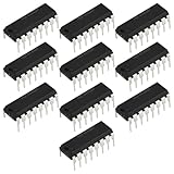
- Component Type: Compatible with HEF4046BP micropower phase-locked loop integrated circuit in DIP16 package for through-hole mounting applications.
- Core Function: Designed for frequency synthesis, signal demodulation, tone decoding, and clock recovery in electronic control circuits.
- Low Power Design: Micropower characteristics make it suitable for battery-operated and energy-efficient frequency or signal control systems.
- Package Style: DIP16 through-hole package allows easy installation, replacement, and prototyping on standard circuit boards and sockets.
- Application Areas: Commonly used in communication equipment, signal processing modules, waveform generation, and timing control circuits.
How to choose a clock-distribution IC
Start with the clocks the system must deliver and the timing error the receivers can tolerate. Compare candidate devices against the full signal path, not just an attractive headline jitter value.
- Frequency plan: Check reference input and oscillator/VCO limits, the required output frequencies, and whether the device supports the necessary integer or fractional multiplication and division.
- Outputs and interfaces: Confirm output count, signaling standards, load requirements, and whether the available outputs can be configured independently as needed.
- Timing adjustment and synchronization: Look for deterministic phase adjustment, reset or sync controls, and feedback inputs if the system needs repeatable alignment or zero-delay operation.
- Noise and loop behavior: Compare phase-noise curves, additive jitter, and loop-bandwidth options. Check the reference quality and the jitter integration limits and measurement method behind each quoted value.
- Implementation constraints: Review integrated versus external loop-filter requirements, supply sensitivity, package and thermal behavior, and the power-integrity needs of the board.
- Acquisition: Check lock-time specifications and their conditions, especially if the design changes frequency or must recover quickly after reset.
Build a system jitter budget that includes the reference, PLL, power-distribution network, crosstalk, termination, and interconnect. Datasheet jitter is condition-dependent: compare like measurement bandwidths, reference quality, output configuration, and test methods. If those conditions differ or are unspecified, the numbers may not be directly comparable.
Rank #4
AD9511 as a documented example
Analog Devices’ 2020 AD9511 datasheet documents a 1.2 GHz clock-distribution IC with a PLL core, reference inputs up to 250 MHz, coarse phase adjustment, and LVPECL plus LVDS/CMOS outputs. It lists five programmable integer dividers, each configurable from divide-by-1 through divide-by-32, and specifies 225 fs rms additive output jitter. The 225 fs figure is a datasheet specification, not a guarantee of total system jitter; evaluate it using the datasheet’s measurement conditions and the planned reference, loop, output, and board configuration. These documented specifications identify the device’s capabilities, but do not establish its current marketplace availability.
Quick Recap
Best Value

- The CD4046B CMOS Micropower Phase-Locked Loop (PLL) consists of a low-power, linear voltage-controlled oscillator (VCO) and two different phase comparators having a common signal-input amplifier and a common comparator input.
- Very low power consumption: 70 µW (typ.) at VCO, VCO inhibit control for ON-OFF keying and ultra-low standby power consumption fo = 10 kHz, VDD = 5 V, Source-follower output of VCO control input (Demod. output), 100% tested for quiescent current at 20 V
- Operating frequency range up to 1.4 MHz (typ.) at VDD = 10 V, RI = 5 k, High VCO linearity: <1% (typ.) at VDD = 10 V, 5-V, 10-V, and 15-V parametric ratings
- Low frequency drift: 0.04%/°C (typ.) at VDD = 10 V, Choice of two phase comparators: Exclusive-OR network (I) Edge-controlled memory network with phase-pulse output for lock indication (II), Zener diode to assist supply regulation, Standardized, symmetrical output characteristics, Meets all requirements of JEDEC Tentative Standard No. 13B, "Standard Specifications for Description of 'B' Series CMOS Devices"
- A Versatile Building Block for Micropower Digital and Analog Applications, Example Applications: FM demodulator and modulator, Frequency synthesis and multiplication, Frequency discriminator, Data synchronization, Voltage-to-frequency conversion, Tone decoding, FSK - Modems, Signal conditioning,
Validate the design before relying on the timing budget
- Specify the system: Record reference and output frequencies, receiver timing limits, required phase relationships, startup behavior, and the target measurement plane. Allocate jitter and skew budgets across the reference, IC, board, and loads.
- Simulate the PLL: Evaluate loop bandwidth, reference choice, phase noise, frequency steps, and spurs with a suitable PLL design tool. Analog Devices recommends ADIsimPLL simulations based on system requirements.
- Build with controlled signal paths: Use clean supplies, appropriate output termination, and controlled differential routing where applicable. For zero-delay designs, match the feedback and output paths to the intended target plane.
- Measure the assembled system: Check phase noise or jitter, lock time, output skew, and sensitivity to supply and load changes at the relevant measurement points.
- Record test conditions: Preserve instrument setup, bandwidth, reference quality, output loading, and board configuration so measured results can be reproduced and compared fairly with specifications.
Product prices and availability are accurate as of the date/time indicated and are subject to change. Any price and availability information displayed on Amazon at the time of purchase will apply.

