
Do these 3 things before closing this tab:
1Scan for outdated or missing drivers - takes under a minute2Clear out junk files and repair common Windows errors3Fix the driver behind crashes, sound loss and screen glitchesJapan’s widely reported $3.9 billion package for Rapidus was a maximum ¥590 billion in support described by the Ministry of Economy, Trade and Industry (METI) on April 2, 2024. It covered both advanced chipmaking processes and a separate advanced back-end project. Rapidus is pursuing domestic 2 nm logic-chip production, with mass production targeted for 2027; that is a plan, not evidence that production or commercial shipments have begun.
What Japan’s ¥590 billion package covers
The $3.9 billion figure is an approximate U.S.-dollar rendering of ¥590 billion, the combined maximum support amount METI described in April 2024. METI divided it between front-end processes, which form circuitry on a silicon wafer, and back-end work, which includes packaging and related processing.

| Project area | Maximum support described by METI in 2024 | What it covers |
|---|---|---|
| Advanced front-end processes | Up to ¥536.5 billion | Advanced semiconductor manufacturing processes for Rapidus’s effort to produce leading-edge logic chips. |
| Advanced back-end processes | Up to ¥53.5 billion | A new project for advanced back-end processing, including packaging-related work. |
| Combined package | Up to ¥590 billion (about US$3.9 billion in industry coverage) | The two support amounts above, not a separate third allocation. |
“Up to” matters: ¥590 billion describes a maximum support package, not proof that Rapidus received that entire amount as cash at once. The dollar figure is an approximate conversion used in coverage, while the official amounts were stated in yen.
Why Japan is funding Rapidus
Japan is trying to rebuild domestic capacity in advanced logic-chip manufacturing after losing ground in that field. The policy combines process research and development, pilot production, advanced packaging, public investment and private-sector capital. The stated national aim is to secure domestic access to chips for demanding uses such as artificial intelligence and advanced computing.
The Tool Desk
Outbyte Driver Updater FREEFix the driver behind crashes, sound loss and screen glitchesFind Drivers →Outbyte PC Repair FREEClear out junk files and repair common Windows errorsFree Scan →Rapidus was founded in 2022. In December 2022, it announced a partnership with IBM to develop 2 nm technology. The project is therefore both a manufacturing effort and a technology-development program: Japan is backing a company intended to develop a domestic route to leading-edge logic production, rather than subsidizing a chip already available to consumers.
When Rapidus says it will make 2 nm chips
Rapidus has set a 2027 target for mass production of 2 nm logic semiconductors. The company reiterated that objective in its February 27, 2026 funding announcement, describing the financing as support for moving from research and development toward mass production. The target is a forward-looking plan; the cited announcements do not establish that mass production has started or that commercial products have shipped.
Rank #2

- IC Type: Semiconductor
- Each wafer fragment contains visible integrated circuit patterns for demonstration and display purposes only.
- Made from single-crystal silicon wafer material for authentic semiconductor teaching and research.
- Ideal for electronics courses, microfabrication demonstrations, and STEM student projects.
- Also suitable for art installations, photography props, and chip design exhibitions.
“2 nm” is a process-node designation for a generation of semiconductor manufacturing, not a claim that every feature on a chip measures exactly two nanometers. The 2024 package’s separate front-end and back-end allocations reflect that producing advanced chips involves both making the circuitry and handling processes such as packaging.
Independent reader supportYour contribution helps us test, update, and keep practical guides available for everyone.How the later financing relates to the 2024 package
The ¥590 billion package is one part of a continuing support effort. Later announcements describe investments and a funding round, which should not be conflated with the 2024 maximum support amount or added together without accounting for overlap.
Quick wins for a faster PC:
Repair Windows errors before they cause bigger problemsFix Now →Fix the driver behind crashes, sound loss and screen glitchesFind Drivers →Clear out junk files and repair common Windows errorsFree Scan →Rank #3
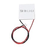
- Semiconductor thermoelectric chip TGM-199-1.4-0.8
| Date | Announcement | How to interpret the figure |
|---|---|---|
| November 21, 2025 | METI selected Rapidus as an eligible operator under the Act on Facilitation of Information Processing and said it intended to invest ¥100 billion through the Information-technology Promotion Agency (IPA), using the fiscal 2025 initial budget. | An intended public investment associated with the selection, separate from the 2024 package. |
| February 27, 2026 | Rapidus announced ¥267.6 billion in combined government and private-sector funding, including a ¥100 billion IPA investment. | A combined funding announcement; the ¥100 billion IPA investment is included in this figure, so it should not be added to it again. |
| June 5, 2026 | IPA announced an additional ¥150 billion equity investment in Rapidus. | A separately announced later equity investment. The announcement does not, by itself, establish a single cumulative total for every form of support and funding. |
These amounts describe different things: a maximum support package, an intended investment, a mixed government-and-private funding figure, and a later equity investment. The announcements do not provide a basis for treating their simple sum as a definitive total invested in Rapidus. In particular, the ¥100 billion IPA investment appears within the ¥267.6 billion February funding figure.
Quick Recap
Best Value

- AUTHENTIC BARE DIE APPEARANCE-- Displays the exposed structure of a semiconductor die before final packaging, providing a direct view of chip layout and microelectronic design features.
- INTEGRATED CIRCUIT REFERENCE SAMPLE --Features visible IC circuitry and semiconductor architecture, making it a useful reference piece for understanding chip manufacturing concepts.
- IDEAL FOR TECHNICAL EDUCATION --Suitable for engineering courses, electronics training, semiconductor learning and STEM activities where physical examples support technical instruction.
- DISPLAY AND PRESENTATION USE --Can be incorporated into technology exhibitions, laboratory displays, classroom demonstrations and microelectronics presentations.
- COLLECTIBLE TECHNOLOGY ARTIFACT-- Combines semiconductor engineering with visual appeal, making it suitable for collectors, electronics enthusiasts and technology-themed displays.
Rank #4

- AUTHENTIC BARE DIE APPEARANCE-- Displays the exposed structure of a semiconductor die before final packaging, providing a direct view of chip layout and microelectronic design features.
- INTEGRATED CIRCUIT REFERENCE SAMPLE --Features visible IC circuitry and semiconductor architecture, making it a useful reference piece for understanding chip manufacturing concepts.
- IDEAL FOR TECHNICAL EDUCATION --Suitable for engineering courses, electronics training, semiconductor learning and STEM activities where physical examples support technical instruction.
- DISPLAY AND PRESENTATION USE --Can be incorporated into technology exhibitions, laboratory displays, classroom demonstrations and microelectronics presentations.
- COLLECTIBLE TECHNOLOGY ARTIFACT-- Combines semiconductor engineering with visual appeal, making it suitable for collectors, electronics enthusiasts and technology-themed displays.
What the announcements do—and do not—show
- They show a sustained public commitment. The 2024 support package and subsequent METI and IPA announcements indicate that the effort continued beyond the initial package.
- They show a production objective, not a completed outcome. Rapidus’s 2027 mass-production target is a plan; the cited figures do not verify achieved volume production or retail chip availability.
- They do not give one clean cumulative investment total. The figures include different support and investment instruments, and at least one later amount is explicitly included in another announcement.
- They do not describe a consumer product subsidy. The funding is for an industrial semiconductor project, including manufacturing and back-end process development.
Product prices and availability are accurate as of the date/time indicated and are subject to change. Any price and availability information displayed on Amazon at the time of purchase will apply.

