
What’s actually slowing this PC down?
Pick the symptom - the matching free tool is one click away.
You can use external PSRAM with STM32 HAL, but there is no universal setup: the right driver and initialization depend on the exact STM32 part and whether the memory connects through FMC, QUADSPI, OCTOSPI, HSPI, XSPI, or HyperBus. First confirm that the MCU supports the memory’s protocol and required read/write behavior; then initialize the device, map or access its address window, and configure startup, cache, and DMA handling.
What PSRAM is—and what it is not
Pseudo-static RAM (PSRAM) is volatile memory with a DRAM core and built-in refresh management, presented through a simpler external interface. It can add working memory when a microcontroller’s internal SRAM is insufficient. Its contents are lost when power is removed; any retention behavior in a low-power mode is specific to the memory and system design.
PSRAM is not interchangeable with every external memory. SPI and QSPI PSRAM use serial command protocols; Octo-SPI PSRAM uses a wider serial interface; HyperRAM uses HyperBus; and parallel PSRAM connects through a memory controller such as FMC. SDRAM requires its own controller configuration and refresh management. NOR flash is nonvolatile storage, not RAM. Even when a peripheral maps PSRAM into the processor’s address space, accesses have different latency, bus behavior, and sometimes write restrictions than internal SRAM.
Identify the STM32 interface before choosing memory
Do not assume that every STM32 supports PSRAM, or that a peripheral name alone proves compatibility. Verify the exact MCU part number, package, reference manual, datasheet, board schematic, and Cube firmware package. Check bus width, STR or DTR support, DQS/RWDS, memory-mapped read and write support, clock limits, voltage, address range, and DMA routing.
Do these 3 things before closing this tab:
1Repair Windows errors before they cause bigger problems2Scan for outdated or missing drivers - takes under a minute3Clear out junk files and repair common Windows errors#1 Best Overall

- Ultra-low-power with FPU ARM Cortex-M4 MCU 80 MHz with 1 Mbyte Flash, LCD, USB OTG, DFSDM
- On-board ST-LINK/V2-1 debugger/programmer with SWD connector
- Can be powered from USB
- Three LEDs, Two Push-buttons
- Support of wide choice of Integrated Development Environments (IDEs) including IAR, ARM Keil, GCC-based IDEs
| STM32 interface | Typical memory | HAL family or API | Practical consideration |
|---|---|---|---|
| FMC SRAM bank | Parallel asynchronous or synchronous PSRAM/CRAM | HAL_SRAM_* |
SRAM-like address access, but uses more pins; timing must match the device. |
| QUADSPI | SPI or QSPI PSRAM | HAL_QSPI_* |
Lower pin count; capabilities and memory-mapped write behavior vary by MCU. |
| OCTOSPI | Octal-SPI PSRAM, HyperRAM on supported parts, and some narrower serial memories | HAL_OSPI_* in traditional Cube HAL |
Supports wider serial modes on suitable devices; DQS and timing configuration may matter. |
| HSPI | Serial memories supported by the particular STM32U5 variant | HAL_HSPI_* or a newer abstraction, depending on package |
Do not assume a U5 board uses OCTOSPI; check the board schematic and MCU documentation. |
| XSPI | Supported external memories on newer devices such as STM32H7RS | HAL_XSPI_* in applicable HAL generations |
Use documentation and examples for the exact MCU and HAL release. |
ST’s external serial-memory interoperability guide describes these interface families; ST’s AN5050 covers Octo-SPI, Hexadeca-SPI, and XSPI configuration examples. For FMC, ST’s SRAM HAL documentation explicitly includes PSRAM among supported memory types. Confirm all capabilities against your specific part and package.
Choosing an interface
- FMC: Consider it when suitable FMC pins are available and SRAM-like accesses or predictable external-bus transactions matter more than pin count.
- QSPI: Consider it when pin count is tight and the target workload can tolerate serial-memory latency. Check that the MCU supports the required write mode.
- OCTOSPI: Consider it when the MCU supports the selected protocol and the board can route the wider bus and any required DQS signals.
- HyperBus: Use only with a HyperBus-capable peripheral and a compatible memory and board. It is not simply QSPI with eight data pins.
- SDRAM: Consider it for larger or sustained high-throughput workloads when FMC SDRAM support and board pins are available.
- Internal SRAM: Prefer it for latency-critical data, interrupt state, DMA descriptors, and objects needed before external-memory initialization.
Check the memory and board before configuring CubeMX
Read the memory datasheet alongside the MCU reference manual and board schematic. A family name is not enough: the exact part suffix can change voltage, package, temperature grade, and signaling. AP Memory’s SPI/QSPI product listing, for example, includes devices with different densities and voltage variants. Verify these items before writing initialization code:
- Supply and I/O voltage compatibility; determine whether level shifting is needed.
- Package, footprint, pinout, bus width, and the actual alternate-function pins routed on the board.
- Chip select, clock, data lines, reset, and DQS/RWDS where applicable.
- For FMC, address and data wiring, byte lanes, and the chosen bank.
- Power-up and reset behavior, required configuration-register writes, latency settings, and burst or wrap modes.
- Clock frequency, STR/DTR mode, dummy cycles, sample shifting or delay block, and DQS configuration.
- Signal-integrity and routing requirements for the selected memory and speed.
CubeMX can generate peripheral, clock, and GPIO scaffolding, but that does not necessarily configure the memory’s vendor-specific reset sequence, latency registers, read/write commands, or operating mode. ST also notes in AN5050 that pins may require manual configuration when the selected connection does not match CubeMX’s suggested setup.
Rank #2

- Experience unrivaled performance with the STM32H723ZGT6 core board, featuring a blazing 550MHz main frequency for seamless operation
- Harness the power of 1MB Flash and 564K SRAM on the STM32H723 development board, ensuring ample storage and memory for your projects
- Seamlessly expand your capabilities with the external W25Q64, boasting 8M bytes of capacity on the STM32H723 core board system learning board
- Effortlessly navigate through tasks with the convenient Type C interface, SPI LCD, and 108 IO ports on the STM32H723 core board
- Elevate your development experience with the STM32H723 core board, equipped with a screen interface and camera port for enhanced functionality
Configure the peripheral and initialize the PSRAM
FMC parallel PSRAM
In CubeMX, enable the FMC bank connected to the memory, assign the correct pins, and set the bus width and timing based on the device datasheet and MCU timing limits. FMC PSRAM configuration commonly involves address/data multiplexing, memory type, write operation, wait signals, extended mode, and separate read/write timing where the hardware and memory require them.
Recommended Free Tools
The following is a representative legacy Cube HAL pattern, not portable copy-and-paste code. Structure fields and available options vary between STM32 families and HAL generations; confirm them in the generated project and the selected device’s documentation.
SRAM_HandleTypeDef hsram;
FMC_NORSRAM_TimingTypeDef timing = {0};
FMC_NORSRAM_TimingTypeDef ext_timing = {0};

hsram.Instance = FMC_NORSRAM_DEVICE;
hsram.Extended = FMC_NORSRAM_EXTENDED_DEVICE;
hsram.Init.NSBank          = FMC_NORSRAM_BANK1;
hsram.Init.DataAddressMux  = FMC_DATA_ADDRESS_MUX_DISABLE;
hsram.Init.MemoryType      = FMC_MEMORY_TYPE_PSRAM;
hsram.Init.MemoryDataWidth = FMC_NORSRAM_MEM_BUS_WIDTH_16;
hsram.Init.WriteOperation = FMC_WRITE_OPERATION_ENABLE;

/* Set remaining Init and timing fields for the exact MCU and PSRAM. */
if (HAL_SRAM_Init(&hsram, &timing, &ext_timing) != HAL_OK) {
    Error_Handler();
}
Set access timing from the PSRAM’s timing requirements and the FMC clock, allowing for the exact board and operating conditions. Once FMC is initialized, accesses use the bank’s memory window. Obtain the base address from the MCU reference manual and bank configuration; there is no universal STM32 FMC base address.
Rank #3
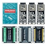
- 【ESP32-S3 PERFORMANCE】Dual-core 240MHz processor with 16MB Flash and 8MB PSRAM for IoT, AI, and machine learning projects.
- 【WIRELESS CONNECTIVITY】Onboard antenna for 2.4GHz WiFi and Bluetooth 5.0 LE — for smart home devices, no external antenna needed.
- 【LEAD-FREE GOLD EDITION DESIGN】Immersion gold (ENIG) plating for durability and conductivity. Lead-free, RoHS-compliant — for long-term prototyping.
- 【PRE-SOLDERED, PLUG-IN DESIGN】ESP32-S3 boards come with pre-soldered headers and plug directly into the included expansion and terminal boards — no soldering required.
- 【MULTI-PLATFORM COMPATIBILITY】Works with C++, MicroPython, ESP-IDF, Raspberry Pi, and STM32 — with online tutorials for quick start. Power via USB-C (5V) or VIN pin (5–12V); do not exceed 5V on the USB-C ports.
QSPI and OCTOSPI regular-command PSRAM
For a regular-command serial PSRAM, the transaction definition must match the datasheet: instruction, address, optional alternate or mode bytes, dummy cycles, and data phase. The device datasheet also determines bus width per phase, address length, reset and configuration commands, latency, and burst behavior. The general initialization order is:
- Initialize clocks and GPIO alternate functions, then initialize the family-specific HAL peripheral.
- Send the memory’s documented reset sequence, if required.
- Write configuration registers for latency, burst/wrap behavior, or other required settings.
- Configure separate read and write command templates with the correct opcode, address, bus widths, dummy cycles, and STR/DTR settings.
- Enter memory-mapped mode if the selected peripheral and memory combination supports the access pattern you need.
In traditional Cube HAL, the conceptual OSPI calls resemble HAL_OSPI_Init(), device-specific calls using HAL_OSPI_Command(), and HAL_OSPI_MemoryMapped(). The command structures are device-specific. Enabling memory-mapped mode configures the STM32 peripheral; it does not identify or initialize the PSRAM automatically. For some combinations, indirect transactions may be needed, especially if the required memory-mapped write operation is unsupported.
HyperRAM and HyperBus
HyperRAM uses HyperBus transactions rather than ordinary SPI command opcodes. Depending on the device and board, the implementation may require an 8-bit data bus, clock wiring, RWDS/DQS, reset handling, and device-specific latency settings. Select HyperBus mode only when both the STM32 peripheral and memory support it, then follow the memory datasheet and the relevant STM32 example. ST’s AN5050 documents an Infineon HyperRAM/HyperFlash MCP example separately from its Quad-SPI and Octo-SPI PSRAM examples.
Rank #4

- Memory: W25Q16
- High-frequency crystal oscillator: 8 MHz
- Low-frequency crystal oscillator: 32.768 kHz
- 2.54 mm pin pitch
- STM32F407VET6: 512 KB Flash
Newer XSPI HAL APIs
ST’s HAL2 XSPI use-case documentation presents a flow using HAL_XSPI_SetConfigIOManager(), HAL_XSPI_Init(), HAL_XSPI_SetConfig(), HAL_XSPI_SendRegularCmd(), and HAL_XSPI_StartMemoryMappedMode(). See the ST HAL XSPI use cases. This API applies to its documented HAL generation and device support; do not mix it with legacy HAL_OSPI_* code without checking the selected Cube package.
Bring up the memory in stages
- Check compatibility: Confirm the MCU protocol, memory voltage and pinout, board routing, and reset requirements.
- Start conservatively: Begin with a low memory clock and the simplest supported signaling mode.
- Initialize the interface: Enable clocks, configure GPIO, and call the appropriate FMC, QSPI, OSPI, HSPI, or XSPI initialization function.
- Initialize the device: Send the exact reset and configuration transactions from its datasheet. Use indirect mode first when available.
- Verify communication: Read a documented register or ID if the device provides one; otherwise use a small transaction test appropriate to its protocol.
- Test basic accesses: Test aligned 8-, 16-, and 32-bit accesses as supported by the memory window, then multiple addresses and nonzero data patterns.
- Test blocks and mapping: Run sequential and varied-pattern tests, then enter memory-mapped mode and repeat.
- Test integration: Add linker placement, MPU/cache policy, and DMA tests separately so a failure can be isolated.
- Increase speed carefully: Change one timing or clock setting at a time and repeat the tests.
#include <stdint.h>
#include <stddef.h>

#define EXT_PSRAM_BASE /* use the address for this MCU and configuration */
#define TEST_WORDS 1024U

static int psram_test(void)
{
    volatile uint32_t *ram = (volatile uint32_t *)EXT_PSRAM_BASE;

    for (size_t i = 0; i < TEST_WORDS; ++i) {
        ram[i] = 0xA5000000u ^ (uint32_t)i;
    }

    for (size_t i = 0; i < TEST_WORDS; ++i) {
        if (ram[i] != (0xA5000000u ^ (uint32_t)i)) {
            return -1;
        }
    }
    return 0;
}
Replace the base-address definition with the mapped address for the exact STM32 peripheral configuration. A passing CPU test does not prove that DMA, cache coherency, or high-speed operation is correct.
Place application buffers in external memory safely
Add a dedicated region to the linker script using the actual mapped address and fitted memory capacity. This example leaves both values intentionally device-specific:
Free tools Windows power users keep installed
One-click scans. No signup required.
Best Value

- STM32F103C8T6 ARM STM32 minimum system development module.
- ST-Link V2 support the full range of STM32 SWD interface debugging, simple interface (including power supply), 4 line speed, stable work.
- Use the current smart phones of Mirco USB interface, easy to use, USB communication and power supply can be done.
- The board lead to all the I/O resources.Download with SWD debug interface, which requires a minimum of 3 wires to complete debug a download task
MEMORY
{
  /* Keep the project's existing regions and values. */
  EXT_PSRAM (xrw) : ORIGIN = 0xXXXXXXXX, LENGTH = 8M
}

.ext_psram (NOLOAD) :
{
  . = ALIGN(32);
  *(.ext_psram*)
  . = ALIGN(32);
} > EXT_PSRAM
Use NOLOAD for volatile buffers that do not need initialization from flash. Match the region length to the installed device and reserved address window, not just a product family’s nominal density. A selected buffer can be placed in the section like this:
__attribute__((section(".ext_psram"), aligned(32)))
uint8_t frame_buffer[800 * 480 * 2];
The section must not be read or initialized by startup code before PSRAM is ready. Keep .data, the stack, heap, C++ static initialization, and RTOS objects in internal memory until initialization order and early access have been verified. A safer initial design is to initialize PSRAM explicitly, then allocate or use external buffers.
Set cache and MPU policy before sharing buffers with DMA
On STM32 cores with data cache, the CPU may hold a different view of memory from a DMA engine. A CPU test can pass while a peripheral transfer sees stale data or the CPU later reads stale cache lines. Choose an MPU/cache policy deliberately and follow the core-specific documentation:
| Policy | Benefit | Trade-off |
|---|---|---|
| Non-cacheable region | Simplifies CPU/DMA visibility. | CPU accesses can be slower. |
| Write-through | Can simplify visibility for CPU writes. | Writes still go to external memory and performance may be lower. |
| Write-back | Can improve CPU performance. | Requires correct cache maintenance and ownership rules. |
| Separate DMA buffers | Makes transfer ownership easier to manage. | May require additional memory or copying. |
For cacheable buffers, clean cache lines before DMA reads data written by the CPU, and invalidate the relevant lines after DMA writes data that the CPU will read. Align buffer addresses and lengths to the core’s cache-line requirements, and avoid accessing the same physical memory through aliases with different cache attributes. Consult the reference manual for whether the chosen DMA controller or MDMA can access the external memory region and which request path applies. Test external-RAM-to-peripheral and peripheral-to-external-RAM directions separately, then test concurrent CPU/DMA access.
Diagnose common failures
Reads return the same value or do not change
- Likely causes: Memory-mapped mode was not entered; the address is wrong; chip select, reset, voltage, GPIO alternate function, protocol, opcode, or address width is incorrect; or the device was not initialized.
- Next checks: Verify power and signals at the memory, confirm the mapped address, try the documented indirect command path, read a supported ID or register, and reduce clock speed.
Reads work but writes fail
- Likely causes: The selected MCU/protocol combination does not support the needed memory-mapped writes, the write command is absent or incorrect, device configuration is incomplete, or latency and STR/DTR settings do not match.
- Next checks: Confirm write support in the exact MCU documentation and test writes through indirect mode. ST community guidance discusses restrictions for some STM32H7 QUADSPI SDR-PSRAM scenarios and distinguishes them from other protocol choices; treat that guidance as a prompt to verify the exact part, not a universal rule. See the STM32H7 memory-mapped QSPI RAM discussion.
Works slowly but fails at the target clock
- Likely causes: Dummy-cycle mismatch, missing DQS, unsuitable sampling or delay settings, trace skew, excessive loading, drive strength, clock mode, voltage, or board signal integrity.
- Next checks: Reduce the clock, begin with STR where supported, check the datasheet timing, tune sample shifting or delay blocks, and validate signals with suitable measurement equipment.
CPU accesses pass but DMA corrupts data
- Likely causes: Stale cache lines, misalignment, inaccessible address region, incorrect DMA request routing, or concurrent access races.
- Next checks: Try a non-cacheable MPU region diagnostically, apply cache maintenance, verify DMA reachability in the MCU documentation, and define clear buffer ownership during transfers.
The system faults during startup
- Likely causes: Startup code, the C runtime, heap, stack, or static initialization touches PSRAM before clocks and the memory interface are ready.
- Next checks: Keep startup-critical objects internal, use a non-loaded external section, and initialize PSRAM before creating or using external buffers.
A reference board works but a custom board does not
- Likely causes: Different alternate-function routing, wiring, voltage variant, footprint, reset/power sequence, missing DQS/RWDS, or layout constraints.
- Next checks: Compare the custom schematic and fitted suffix against the working board; do not assume a reference board’s memory population or solder configuration applies to your design.
Use reference designs without assuming they are universal
ST’s AN5050 documents examples on the STM32L4P5G-DK using AP Memory APS6408L-30B-BA Octo-SPI PSRAM, AP Memory APS1604M-3SQR Quad-SPI PSRAM, Macronix Octo-SPI flash, and an Infineon HyperRAM/HyperFlash MCP. These are board-specific examples, not a generic pin map or initialization recipe. The STM32L4P5G-DK data brief describes its MCU and onboard memory resources. For another useful reminder that peripheral assignment is board-specific, ST community guidance notes that the STM32U5A9J-DK PSRAM connects to HSPI1 rather than OCTOSPI1: U5A9J-DK HSPI/PSRAM discussion.
Quick Recap
Product prices and availability are accurate as of the date/time indicated and are subject to change. Any price and availability information displayed on Amazon at the time of purchase will apply.

