
Quick wins for a faster PC:
Clear out junk files and repair common Windows errorsFree Scan →Scan for outdated or missing drivers - takes under a minuteDriver Scan →Repair Windows errors before they cause bigger problemsFix Now →iTechGuides is reader-supported. When you buy through links on our site, we may earn an affiliate commission. As an Amazon Associate I earn from qualifying purchases. Learn more
Yes. Semiconducting carbon nanotubes can be dispersed in liquid inks and printed into thin-film transistor channels. Researchers are exploring them for flexible electronics, sensors, and display backplanes. But a printable material or promising prototype is not proof of uniform, low-cost mass production: purity, film consistency, processing, and scale remain important hurdles.
What is carbon nanotube electronic ink?
It is a liquid formulation containing dispersed carbon nanotubes that can be deposited as a thin film or patterned feature. For transistor channels, the relevant material is usually semiconducting single-walled carbon nanotubes (SWCNTs). The tubes form a network in the finished film, so the behavior of that network is not necessarily the same as the behavior of an isolated nanotube.

That distinction matters because metallic nanotubes mixed into a semiconducting network can interfere with transistor switching. Ink formulation and the way it is deposited and processed therefore affect the finished device, not just how easily the liquid can be printed. A 2020 review of printed CNT thin-film transistors discusses the materials and progress toward applications (Royal Society of Chemistry, 2020).
Can carbon nanotubes be printed into electronic circuits?
They can be printed into transistor-channel films in research and prototype devices. A 2015 perspective describes semiconducting SWCNTs as compatible with inkjet and aerosol-jet printing, while noting that graphene inks are more suited to electrodes and interconnects in the systems it discusses (American Chemical Society, 2015).
#1 Best Overall
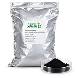
- DEFINED SIZE RANGE — Industrial-grade multi-walled carbon nanotubes with a specified outer diameter of 10-20 nm and length of 20-100 μm.
- GREATER THAN 95 WT% PURITY — Supplied as a fine black powder in a sealed 100 g aluminum foil pouch for laboratory research and industrial materials development.
- MULTI-WALLED TUBULAR STRUCTURE — MWCNTs consist of multiple concentric graphitic carbon walls surrounding a hollow tubular core. The structural graphics shown in the product images are conceptual illustrations and are not microscopy data.
- MATERIAL DEVELOPMENT APPLICATIONS — Suitable for evaluation in polymer and rubber composites, battery and supercapacitor electrodes, conductive inks and coatings, thermal interface materials, sensors and catalyst-support research.
- FORMULATION TESTING REQUIRED — Final conductivity, mechanical reinforcement, thermal behavior and dispersion depend on nanotube loading, dispersion method, matrix chemistry and processing conditions. Use suitable engineering controls and PPE when handling nanotube powders.
Printing is attractive when depositing material onto flexible or large-area substrates is useful. However, compatibility with a printing method does not by itself establish production readiness. Device demonstrations, integrated prototypes, manufacturing demonstrations, and commercial deployment are different levels of evidence.
What could nanotube inks be used for?
Flexible and large-area electronics
Printed CNT thin-film transistors are being explored for electronics on flexible substrates and across large areas. Their potential fit comes from combining semiconducting behavior with deposition approaches that can pattern thin films.
Rank #2

- Product name:High conductivity graphene/carbon nanotube composite slurry
- Graphene content:9.5±0.5 wt%
- Additive content:1±0.1wt%
- Solvent:water
- Conductivity:400-600 S/cm (four-probe method)
Sensors and display backplanes
Review literature identifies sensors and display backplanes as potential application areas. These are prospective uses, not evidence that CNT inks are already widely deployed in commercial products. More complex systems also require successful integration of the printed material with other device components.
The Tool Desk
Outbyte PC Repair FREEClear out junk files and repair common Windows errorsFree Scan →Outbyte Driver Updater FREEScan for outdated or missing drivers - takes under a minuteDriver Scan →Why does a nanotube network perform differently from a single tube?
In a transistor film, many nanotubes form a random network. Electrical performance depends on how that network is composed and deposited, including the tubes’ length, diameter, and density, as well as residual metallic-tube content.
A 2011 American Chemical Society review reported individual nanotube mobility in the 10,000 cm²/V·s range and random-network mobility around 100 cm²/V·s in the work it reviewed (American Chemical Society, 2011). These are historical values summarized by that review, not current commercial-ink specifications or guaranteed device results. They illustrate why performance figures for an individual nanotube should not be assumed to describe a printed network.
Metallic tubes are another concern: their presence can reduce a transistor’s on/off ratio, a measure of how well the device distinguishes its conducting and nonconducting states. The effect depends on the material and device, so a useful comparison needs to state the purity and device architecture along with the reported electrical metrics.
Rank #4

- Conductive film made from advanced carbon nanotube and graphene technology for superior conductivity.
- Ultra-thin devise with a thickness of 0.05-0.1mm, ideal for various applications requiring minimal space.
- Wide temperature range of -40 to 80℃, ensuring reliability in extreme conditions for diverse environments.
- Versatile pH compatibility from 0 to 14, making it suitable for a variety of chemical applications.
- Customizable options available to meet specific project requirements; us for tailored solutions.
Why aren’t printed nanotube transistors widely used yet?
The gap between a working device and a repeatable manufacturing process involves more than printing a conductive or semiconducting film. Reviews identify practical formulation, drying time, film uniformity, scalability, and cost as concerns. A later review focused on large-area active-matrix applications also flags density variation during extended printing and long-term shelf stability as challenges for consistent devices (Journal of Information Display, 2021).
Recommended Free Tools
These issues can interact. Changes in nanotube density or film uniformity can affect device-to-device behavior; storage and post-processing can shape how reliably a formulation performs. Potentially lower cost or mass production should therefore be treated as a goal or possible advantage, not as an established outcome without manufacturing evidence.
Best Value

- Excellent Electrical and Thermal Conductivity
- Excellent Adhesion
- Durable yet Flexible when cured
- Anti-cracking
How to evaluate a CNT ink or printed-device claim
When comparing formulations, research results, or production claims, look for the details that connect material quality to repeatable device performance:
- Semiconducting purity: Is the ink’s residual metallic-tube content reported?
- Nanotube characteristics: Are tube length, diameter, and deposited-network density specified?
- Printing and substrate: Which printing method and substrate were used, and are they compatible with the formulation?
- Device metrics: Are mobility and on/off ratio reported with the device architecture and test conditions?
- Process and consistency: Are drying, post-processing, film uniformity, extended-printing variation, and storage stability addressed?
- Evidence level: Is the claim based on material characterization, one device, an integrated prototype, a manufacturing demonstration, or commercial deployment?
- Scale and cost: Are these demonstrated for a production process, or presented as expected benefits?
Without those particulars, a headline performance number or a statement that an ink is printable cannot show how a finished device will behave at scale.
Quick Recap
Product prices and availability are accurate as of the date/time indicated and are subject to change. Any price and availability information displayed on Amazon at the time of purchase will apply.
What’s actually slowing this PC down?
Pick the symptom - the matching free tool is one click away.

