
Quick wins for a faster PC:
Scan for outdated or missing drivers - takes under a minuteDriver Scan →Repair Windows errors before they cause bigger problemsFix Now →Fix the driver behind crashes, sound loss and screen glitchesFind Drivers →On December 12, 2000, TSMC and VIA Technologies announced that TSMC had delivered functioning 0.13-micron wafers for VIA’s next-generation Cyrix processors. VIA said it had received the wafers and verified that they worked. The announcement concerned working semiconductor wafers—not finished processors already widely available for purchase.
What did TSMC and VIA announce?
TSMC’s December 12, 2000 announcement, issued from Hsin-Chu, Taiwan, described the wafers as the foundry industry’s first functioning 0.13-micron wafers. That “first” designation is TSMC’s claim in its corporate announcement, not an independently established ranking. Read TSMC’s announcement.

The companies said the wafers were for VIA’s next-generation Cyrix processors. TSMC identified the manufacturing process as CL013LV, its high-performance 0.13-micron variant. The release said the designs were intended for value PCs, notebooks, and information appliances; those were the companies’ target-market claims, not independent assessments of product performance.
Which VIA processor was on the wafers?
TSMC’s announcement did not give a processor model number. A Taipei Times report published December 13, 2000 said a VIA official identified the processor as Samuel II. The model identification therefore comes from the newspaper’s reporting, not from TSMC’s release.
#1 Best Overall

- VIA Desktop CPU Processor
- Model: C3-650MHz
- Socket: PGA370
- Cores: 1
- Frequency: 650 MHz
Contemporaneous EE Times coverage likewise described the wafers as containing VIA’s next-generation x86 processor.
What did TSMC’s CL013LV process mean?
TSMC described its 0.13-micron process family as three options: core CL013G, low-power CL013LP, and high-performance CL013LV. VIA’s processor wafers used CL013LV, so the specifications below are historical vendor specifications for that process generation—not measurements of a retail CPU or an independent comparison with competing processes.
Rank #2
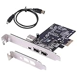
- PCIe IEEE 1394 firewire adapter is backward compatible with devices in 400/200/100Mbps transmission speed; Provide with a low profile bracket and a firewire cable, your best choice of firewire card for PC
- Works with Various Types of 1394a Devices Including Portable Hard Disk, DV Camcorder, Digital Camera, CD-RW/DVD-ROM Drive and Other Audio/Video Devices
- VIA chip, compliant with PCI Express Base Specification 1.0a and compliant with IEEE 1394-1995, 1394a-2000 and OHCI 1.1 Standards
- Plug and Play; It supports Windows 98 SE, ME, 2000, XP, Server 2003, Vista, 7 (32-bit/64-bit), Windows 8, Windows 10, and Mac OS
- No drive required; 1394 devices are built into Windows 98 2nd and above (included) operating systems, It does not need to download driver separately. NOTE: PCIe Firewire 400 Card just provides a channel from the camera to the computer only, the image captured by the camera does not make any modification, if the captured video is not satisfactory, please check the pixel settings of your camera.This model is VIA chip, so it does not support the firewire sound card.Please contact us if you have any questions!
| TSMC-reported feature | Value or qualification |
|---|---|
| Process family options | CL013G (core), CL013LP (low power), and CL013LV (high performance) |
| Core voltage | 1.0 V |
| I/O voltage | 2.5 V or 3.3 V |
| Gate length | 0.08 micron |
| Embedded 6T SRAM cell size | 2.43 µm² |
| CL013LV small ring oscillator delay | 11 picoseconds at 1.2 V |
| CL013LV delay per gate | 14 picoseconds at 1.0 V |
TSMC said its 0.13-micron process was a 72% shrink relative to its 0.18-micron technology, and that the embedded SRAM cell was 52% smaller than its 0.18-micron-process counterpart. These are TSMC’s reported comparisons. In a later historical overview, TSMC characterized its 0.13µm technology as its first 0.13µm low-k, copper SoC process technology; that describes the broader process generation, while the VIA wafers were specifically associated with CL013LV. TSMC’s process overview.
Did the announcement mean a finished CPU was on sale?
No. It reported delivery and verification of functioning wafers. Wafers are an intermediate stage in semiconductor manufacturing; the announcement did not say that finished retail processors were already broadly on sale. VIA CEO Wenchi Chen said the company expected to be the first to launch a CPU using an advanced 0.13-micron process, but that was a forward-looking statement in the companies’ announcement, not confirmation of a retail launch on December 12.
The Tool Desk
Outbyte Driver Updater FREEScan for outdated or missing drivers - takes under a minuteDriver Scan →Outbyte PC Repair FREEClear out junk files and repair common Windows errorsFree Scan →What happened with VIA’s later 0.13-micron processors?
On June 5, 2001, VIA announced that the Ezra version of its VIA C3 was entering volume production on a 0.13-micron process. VIA said Ezra debuted at speeds up to 800 MHz and offered PGA, micro-PGA, and EBGA package options. VIA’s June 2001 announcement.
This later release establishes that a named VIA C3 processor used a 0.13-micron process and entered volume production. The available announcements do not explicitly confirm that Ezra was the same processor model as the wafers TSMC and VIA discussed in December 2000.
Rank #4
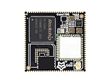
- Part Number: Core110614N256
- Luckfox Core1106 Core Board, 256MB, with Wireless, 256MB SPI NAND, Based On Rockchip RV1106 Chip, Integrates ARM Cortex-A7/RISC-V MCU/NPU/ISP Processors
- RV1106G2 chip, with Wireless, 256MB SPI NAND, NPU 1TOPS, 256MB DDR3L
- The Core1106 is a core board based on the Rockchip RV1106 series chips, featuring high performance and high expandability
- Providing a convenient platform for developers to design their own hardware, enabling quick design verification or direct integration into products, thereby shortening the R&D cycle.
How did TSMC’s 0.13-micron technology scale afterward?
In 2003, TSMC reported that more than 230 product designs had taped out to its 0.13-µm processes and that it had shipped more than 100,000 eight-inch-equivalent 0.13-µm wafers. Those figures describe TSMC’s process business as a whole, not VIA’s processor wafers. TSMC’s 2003 announcement.
Quick Recap
Best Value
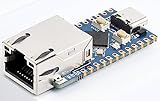
- 【RP2040-ETH Module】 Based On RP2040, Onboard Ethernet Port,Dual-core Arm Cortex M0+ processor, flexible clock running up to 133 MHz 264KB of SRAM, and 4MB of onboard Flash memory.
- Onboard CH9120 with integrated TCP/IP protocol stack. 14 × multi-function GPIO pins, compatible with some Pico HATs.
- Castellated module allows soldering direct to carrier boards. Drag-and-drop programming using mass storage over USB. 8 × Programmable I/O (PIO) state machines for custom peripheral support. Controllable via network.
- Support multiple communication modes: Supports TCP Server / TCP Client / UDP Server / UDP
- Support C/C++, MicroPython, Arduino: Comprehensive SDK, Dev Resources, Tutorials To Help You Easily Get Started
Product prices and availability are accurate as of the date/time indicated and are subject to change. Any price and availability information displayed on Amazon at the time of purchase will apply.
What’s actually slowing this PC down?
Pick the symptom - the matching free tool is one click away.

