
Quick wins for a faster PC:
Repair Windows errors before they cause bigger problemsFix Now →Scan for outdated or missing drivers - takes under a minuteDriver Scan →Clear out junk files and repair common Windows errorsFree Scan →Power in a switching boost converter is lost mainly as heat in the switch and rectifier, inductor, capacitors, and supporting circuitry. The amount lost in each place depends on the converter’s operating point, topology, components, and temperature—there is no universal ranking of loss mechanisms.
Start with the power balance
At steady state, the difference between input power and delivered output power is the converter’s dissipated power:
Power loss = input power − output power
Efficiency is output power divided by input power. For a real design, calculate input and output power at the same line, load, and temperature conditions, then compare the measured difference with an itemized loss estimate. A worked example for one device or operating point is not a general efficiency figure.
Where the losses occur
MOSFET or integrated switch
The switch has conduction loss while it is on and transition loss as it turns on and off. A first-order conduction estimate is the RMS switch current squared multiplied by the switch’s on-resistance and the fraction of the cycle it conducts. Use the actual boost-converter current waveform and the device’s resistance at operating temperature; duty cycle and current vary with input voltage and load.
Do these 3 things before closing this tab:
1Scan for outdated or missing drivers - takes under a minute2Clear out junk files and repair common Windows errors3Fix the driver behind crashes, sound loss and screen glitches#1 Best Overall

- Small size,product size: 22 × 11 × 3.6mm
- Support 5V/8V/9V/12V, the default is 12V
- The front side of the PCB can be seen with the words A and B. The output voltage can be changed by using the soldering iron to change the pad on and off.
During a switching transition, voltage and current overlap. A simplified estimate for one transition is proportional to one-half times voltage, current, and transition time; multiply the estimated energy per transition by switching frequency to estimate average switching loss. Vendor switching-energy data or measured waveforms can give a better estimate than this approximation.
Driving the MOSFET gate also consumes power. A rough gate-drive estimate is gate charge multiplied by drive voltage and switching frequency. Device capacitances and the gate driver’s own consumption can add to the total.
Rank #2
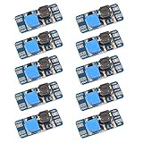
- Mini DC-DC step up voltage regulator with DC 2-24V input and 5V-28V output,just connected with USB power adapter then you can get 9V 12V 18V 24V voltge.
- Equipped with MT3608 voltage booster chip with high conversion efficiency up to 93%.
- Widely used for storage battery, power transformers, DIY adjustable regulated power supply, industrial equipment, 5V, 9V, 12V, 28V output, etc.
- MT3608 includes under-voltage lockout, current limiting, and thermal overload protection to prevent damage in the event of an output overload.
- Note: Before the first use, the module is not powered and not connected to the load, the blue potentiometer copper head a word mouth adjustment cap, aligned with the direction of the chest, counterclockwise rotation of the potentiometer to the end of the "ta" sound, and then clockwise rotation of the potentiometer more than 30 turns, and finally connected to the power supply, using a multimeter to monitor the module's output voltage to achieve the desired voltage
Rectifier diode or synchronous switch
In an asynchronous boost converter, the diode conducts while the main switch is off. Its approximate forward-conduction loss is average forward current multiplied by forward voltage over its conduction interval. The diode can also dissipate energy during reverse recovery, when it stops conducting and briefly carries reverse current.
TI’s boost-converter design note recommends considering Schottky diodes to reduce losses, while still meeting the design’s voltage, current, leakage, and thermal requirements. A synchronous rectifier replaces the diode with a controlled switch and can reduce forward loss, but adds switch conduction and drive losses, timing constraints, and potential dead-time loss. Which approach performs better depends on the design and operating point.
Windows Errors? Fix Them Before They Spread
Repair common Windows errors and clear accumulated junk for a smoother, more stable PC - no reinstall needed.Free scan · no reinstallCrashes, No Sound, or Screen Glitches?
Random freezes, missing sound and display glitches usually trace back to one bad driver. Find and replace yours safely.Free scan · under a minuteRank #3

- XL6009 is a high-performance 400KHz 4A switch currency step-up (BOOST) module. This module is coming with the 3rd generation high-frequency switch technology as the core chip, The performance is much higher than LM2577
- Wide input voltage: 3V~32V;Optimum operating voltage range: 5~32V;Wide output voltage: 5V~35V
- With 4A high efficiency MOSFET switches, the efficiency of XL6009 can be up to 94%(LM2577current is 3A
- With ultra high switch frequency 400KHz , even if small capacity filtering capacitors can achieve very good results, ripple is smaller (Compared to LM2577,its frequency is 50KHz)
- With 0.1uF high-frequency bypass capacitor, effectively filter out high-frequency noise
Inductor winding and core
Winding, or copper, loss is approximately RMS winding current squared multiplied by the inductor’s DC resistance (DCR). Account for the resistance increase with temperature; AC winding effects can also matter at switching frequencies.
Core loss arises from changing magnetic flux. It depends on the core material, flux swing, and switching frequency, so estimating it generally requires manufacturer loss data or a suitable model. A lower-DCR inductor does not necessarily have the lowest total loss: core behavior, current rating, size, and operating frequency also matter.
Rank #4
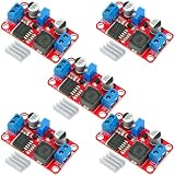
- XL6019 Boost Converter Module:The conversion efficiency can reach over 90%, which is convenient for thermal design
- Size:50*28*13mm
- Current: Maximum: 0-5A; Recommended value 0-3A
- Input: Maximum: 3-40V; Recommended value 3V-35V
- Output: Maximum: 5-45V; Recommended value 5V-40V (by rotating the potentiometer)
Capacitors, board paths, and support circuitry
Ripple current flowing through a capacitor’s equivalent series resistance (ESR) produces heat. Depending on the capacitor and operating conditions, leakage and dielectric losses may matter too. PCB copper, connectors, shunts, and wiring also dissipate power through resistance.
A complete budget includes the controller’s quiescent current, gate-drive supply, bias or regulator consumption, and startup or protection circuitry. These auxiliary loads can take a larger share at light load. Use the specific controller’s datasheet rather than assigning them a generic loss figure.
Best Value

- Boost Converter :Adjustable high power digital booster module
- Size:72*48mm
- Voltage:Input voltage:4-35V;Output voltage:5-45V
- Electric current:5A max
- Compatible with power supplies for laptops or solar panels and other electronic devices digital products etc
How to estimate the total loss
- Define the operating range. Record the input-voltage range, output voltage and current, switching mode, and switching frequency. Identify whether the controller supports continuous-conduction mode (CCM), discontinuous-conduction mode (DCM), or pulse skipping in the conditions you need to evaluate.
- Calculate the operating currents. Determine duty cycle, inductor current, and switch current using boost-specific waveforms. Check the worst-case input voltage and load: TI’s SLVA372D highlights minimum input voltage in maximum-current calculations and relates ripple to input voltage, duty cycle, frequency, and inductance.
- Use realistic component data. Estimate switch conduction with hot on-resistance and RMS current; estimate switching and drive loss from device data or waveforms. Include diode forward and reverse-recovery loss, inductor winding and core loss, capacitor ESR loss, and auxiliary consumption as applicable.
- Add the estimates and measure the converter. After thermal stabilization, measure input voltage and current and output voltage and current at the same operating point. Compare measured input-minus-output power with the sum of estimated component losses. A residual points to missing parasitics, inaccurate assumptions, or model error; it is not itself a measured allocation to any one component.
These are simplified engineering estimates, not substitutes for topology-specific waveforms and device data. The available design guidance does not establish a numeric loss breakdown for a particular converter without its specifications and measurements.
Independent reader supportYour contribution helps us test, update, and keep practical guides available for everyone.Compare design choices at the same conditions
| Choice | Potential benefit | Costs and checks |
|---|---|---|
| Lower-resistance switch | Can reduce conduction loss. | May have greater capacitance and transition loss. Compare both at the intended voltage, current, frequency, and temperature. |
| Diode versus synchronous rectification | A synchronous switch can reduce rectifier forward loss. | It adds drive, conduction, timing, and dead-time losses; diode reverse recovery and forward drop also depend on the selected part and operating conditions. |
| Higher switching frequency | Can allow lower inductance and smaller passive components. | Raises switching loss and can increase magnetic loss. Include ripple, EMI, thermal margin, and voltage/current stress in the comparison. |
| Inductor with lower DCR | Can reduce winding loss. | Evaluate core loss, saturation/current margin, size, cost, frequency, and temperature too; DCR alone does not determine total inductor loss. |
For a boost converter, increasing inductance reduces ripple, but the preferred value is a system tradeoff rather than a universal maximum. TI’s SLVA372D, revised November 2022, states: “The higher the inductor value, the higher is the maximum output current because of the reduced ripple current.” The note also discusses the size benefit of smaller inductance and the need for adequate current rating.
When selecting a boost-converter inductor, match inductance, saturation and current rating, DCR, core behavior, switching frequency, temperature, size, and the intended converter. Compare candidate designs across the same input voltage, load, and thermal conditions rather than optimizing a single datasheet number.
Quick Recap
Sources
- Analog Devices, An Efficiency Primer for Switch-Mode, DC-DC Converter Power Supplies.
- Analog Devices, Small, High-Voltage Boost Converters.
- Texas Instruments, Basic Calculation of a Boost Converter’s Power Stage (SLVA372D), revised November 2022.
- Analog Devices, Inductor Choice Yields Performance Tradeoffs in DC-DC Converters.
- Texas Instruments, Power Loss in Switching Power Supplies.
- Texas Instruments, Conduction Losses in a DC/DC Converter.
Product prices and availability are accurate as of the date/time indicated and are subject to change. Any price and availability information displayed on Amazon at the time of purchase will apply.
Free tools Windows power users keep installed
One-click scans. No signup required.

