
What’s actually slowing this PC down?
Pick the symptom - the matching free tool is one click away.
Start by checking the signal at the IC input pin, not just at its source: verify that its voltage crosses a guaranteed logic threshold cleanly, tie every unused input to a fixed logic level, and add a 0.1 µF supply bypass capacitor close to the chip. Then compare the timing you measure with the correct device’s datasheet conditions. A slow or noisy input can make switching appear mistimed even when the buffer’s propagation delay is within specification.
First identify which device is installed
CD4050B and CD4049UB are related six-channel buffers and level converters, but they do not have the same logic polarity. The CD4050B is noninverting; the CD4049UB is inverting. Check the chip marking and the output polarity your circuit requires before interpreting an apparent timing problem. Texas Instruments lists both devices and their package options on its product page; the detailed limits and conditions are in its combined CD4049UB/CD4050B datasheet, Rev. L, revised February 2026.
Do not assume that voltage limits or timing values are interchangeable between family members. Confirm the specifications for the exact part, supply voltage, temperature range, and circuit connection in use.
Why is my CD4050 triggering randomly?
Check whether the input pin is receiving a clean, valid logic level. At a 5 V supply, TI specifies for the CD4050B a maximum low input voltage (VIL) of 1.5 V and a minimum high input voltage (VIH) of 3.5 V over the listed temperature range. The range between those limits is not a guaranteed high or low state. If a noisy or slowly changing signal dwells there, the output’s switching time may vary or appear erratic.
#1 Best Overall

- CD4049UBE is a hex inverting buffer/converter with high input voltage capability for level shifting
- Logic level conversion and buffer applications requiring high fan-out and voltage level shifting
- Good noise immunity with high input voltage capability allowing interfacing between different logic families
- Six inverting buffers with high input voltage tolerance up to 15V beyond supply voltage
- CMOS to TTL conversion level shifting and high current buffer applications
Measure at the IC pin, where wiring pickup, connector intermittency, or loading can change the signal from what you see at its source. Check its minimum and maximum voltage, noise, and rise and fall shape. The 5 V thresholds above apply to the CD4050B under the datasheet’s stated recommended operating conditions; use the exact device’s specifications for other supplies or for the CD4049UB.
How do I stop false triggers in a CD4049 circuit?
Give every input a defined state
Do not leave unused inputs floating. Connect each unused input to a fixed high or low level that is valid for the circuit. Texas Instruments warns in its datasheet layout guidance: “When using multiple bit logic devices, inputs must never float.” An unconnected input can take an undefined state and make circuit behavior unpredictable.
Rank #2

- Including:CD4001 CD4011 CD4013 CD4017 CD4028 CD4049 CD4050 CD4051 CD4052 CD4053 CD4060 CD4066 CD4069 CD4071 CD4081 CD4093 CD4094 CD40106 CD4511 CD4541 .
- CD4049,CD4050:CMOS Hex Buffer Converters
- CD4052,CD4053:CMOS Single 8-Channel Analog Multiplexer/Demultiplexer
- Maximum input leakage 1 µA at 15V over full tempera-ture range
- NOTE:Exposure to absolute maximum rating conditions for extended periods may affect device reliability
Check the wiring and input source
- Inspect solder joints, connectors, and long input wires for intermittent connections or possible noise pickup.
- Observe the signal directly at the IC pin, including its voltage range and edge shape.
- Verify that the signal source can provide valid logic levels for the chosen part and supply voltage.
These are diagnostic checks, not a guarantee that any one fault is present. The source of a false trigger must be established from the particular circuit and measurements.
What capacitor should I put across the CD4050 supply?
For a single-supply device, TI recommends a 0.1 µF bypass capacitor. Install it as close to the IC’s supply pin as possible; the datasheet says, “The bypass capacitor must be installed as close to the power pin as possible for best results.” Also inspect the supply and ground path while the circuit switches. A bypass capacitor is a sound layout practice, but measurements are needed to determine whether supply disturbance is causing a particular symptom.
Recommended Free Tools
Rank #3

- 12 Values CD40 IC each type 3PCS (36PCS),DIP-14 IC Socket(10PCS),DIP-16 IC Socket(10PCS)
- Includes CD4001BE CD4007UBE CD4011BE CD4013BE CD4017BE CD4051BE
- Includes CD4052BE CD4053BE CD4060BE CD4066BE CD4069UBE CD4093BE
- Chip functions include: Logic Chip, Decade Counter,Unbuffered Hex Inverter,Analog Multiplexers
- Each model comes in a separate package and is individually labeled for easy identification and retrieval, preventing any mix-up.
How to distinguish input-edge problems from propagation delay
Propagation delay is the time between a valid input transition and the corresponding output transition under stated test conditions. TI’s CD4050B AC timing table at 5 V gives low-to-high propagation delay of 70 ns typical and 140 ns maximum, and high-to-low delay of 55 ns typical and 110 ns maximum. Those figures were measured with 20 ns input rise and fall times, a 50 pF load capacitance, and a 200 kΩ load.
Compare your measurements with those values only when the device and conditions are comparable. A slower or noisier input edge, different load, or different supply can change observed behavior; the table is not a promise that every circuit will switch with those delays. In practice, checking the input edge and output load first helps separate input-integrity issues from propagation delay.
Rank #4
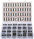
- Big Logic IC Assortment, 46 Types: CD4001, CD4011, CD4013, CD4015, CD4016, CD4017, C4021, CD4022, CD4023, CD4024, CD4025, CD4026, CD4027, CD4028, CD4029, CD4033, CD4042, CD4043, CD4046, CD4047, CD4049UBE, CD4050, CD4051, CD4052, CD4053, CD4060, CD4063, CD4066, CD4069, CD4070, CD4071, CD4072, CD4073, CD4075, CD4077, CD4081, CD4082, CD4093,CD4094, CD4503, CD4511, CD4518, CD4520, CD4541, CD4543, CD4553
- Every IC Type has 2 pcs, CD4017 and CD4049UBE are 4 pcs each
- Includes 10 pcs DIP-14 Sockets and 14 pcs DIP-16 Sockets
- Contains various usefull Logic ICs such as: NOR NAND OR AND Gates, Flip Flop, Shift Register, Bilateral Analog Switch, Decade Octal BCD Binary Counters, R/S Latch, Multivibrator, Hex Inverting Buffer, Multiplexer, Demultiplexer, Comparator, Exclusive Gate, Schmitt Trigger, Timer, PLL, 7-Segment Latch Decoder Driver, Frequency Divider
- Sorted accordingly in a labeled plastic box with pin configuration diagrams
Check voltage limits and loading before changing the circuit
Voltage compatibility matters as well as threshold crossing. TI’s application guidance warns that CD4049UB inputs must remain below VCC because of input clamp diodes, and that outputs must not be pulled above VCC. Output load current must also remain within the selected device’s limits. Verify the exact constraints for the part and implementation rather than assuming the CD4050B and CD4049UB tolerate the same connections.
If the source is inherently slow or noisy, a suitable hysteretic input-conditioning stage or a change to the signal source may be worth considering. The right thresholds and components depend on the actual signal range, supply, noise, timing needs, and downstream circuit; there is no universal resistor network or replacement circuit for an unspecified schematic. Validate changes against the device datasheet and the requirements of the complete implementation.
Do these 3 things before closing this tab:
1Repair Windows errors before they cause bigger problems2Fix the driver behind crashes, sound loss and screen glitches3Clear out junk files and repair common Windows errorsQuick Recap
Best Value

- Logic gate IC chip 10PCS CD4011 CD4001 CD4094 CD4060 CD4069 CD40106 CD4051 CD4052 CD4053 CD4093 CD4013 CD4017 SOP14 SOP16
A practical troubleshooting order
- Confirm the part and supply. Read the device marking, measure VCC at the IC, and verify the correct polarity and voltage limits for the connected circuitry.
- Inspect all input pins. Tie each unused input high or low at a valid level; check used inputs, solder joints, connectors, and long wiring.
- Measure the signal at the IC pin. Check minimum and maximum voltage, noise, and rise and fall times. For a 5 V CD4050B, use 1.5 V maximum for a guaranteed low and 3.5 V minimum for a guaranteed high.
- Check local power integrity. Place a 0.1 µF bypass capacitor close to the supply pin and inspect supply and ground behavior during switching.
- Compare timing under comparable conditions. Account for input edge rate and output loading before drawing conclusions from the datasheet delay values.
- Change input conditioning only with circuit details available. Choose any hysteresis or signal-conditioning solution based on measured signal and noise levels and the downstream requirements.
Product prices and availability are accurate as of the date/time indicated and are subject to change. Any price and availability information displayed on Amazon at the time of purchase will apply.

