
Do these 3 things before closing this tab:
1Clear out junk files and repair common Windows errors2Scan for outdated or missing drivers - takes under a minute3Repair Windows errors before they cause bigger problemsA CD4050B circuit can delay turning a load on; a CD4049UB circuit can delay turning it off. In both examples, a resistor and capacitor create a slowly changing voltage, and the logic chip changes its output when that voltage crosses an input threshold. The resulting delay is approximate—not a calibrated interval—because the threshold and the RC charging behavior vary.
What changes between the CD4050 and CD4049 timer circuits?
The key difference is output polarity. Texas Instruments identifies the CD4050B as a noninverting hex buffer and the CD4049UB as an inverting hex buffer; both have six channels. In the cited circuits, a transistor uses that polarity to control a relay, so the two versions produce opposite load sequences.
| Example | Logic action | Relay and load sequence |
|---|---|---|
| CD4050B on-delay | Noninverting: output goes high after the RC input voltage reaches the switching threshold. | Relay starts de-energized; after the delay, it energizes and the connected load turns on. |
| CD4049UB off-delay | Inverting: output starts high, then goes low when the RC input voltage reaches the switching threshold. | Relay starts energized; after the delay, it de-energizes and the connected load turns off. |
The specific examples and their parts are described by Electronics For You’s CD4050 on-delay and CD4049 off-delay circuits. This polarity difference—not a special timing mode built into either IC—is what makes one arrangement an on-delay and the other an off-delay.
How the RC delay works
At power-up, the timing capacitor C1 is discharged. It charges through a resistor and adjustable potentiometer, so the voltage at the logic input rises gradually rather than changing instantly. When that voltage reaches the chip’s switching threshold, the logic output changes state. The output then controls transistor T1, which switches relay RL1.
#1 Best Overall

- CD4049UBE is a hex inverting buffer/converter with high input voltage capability for level shifting
- Logic level conversion and buffer applications requiring high fan-out and voltage level shifting
- Good noise immunity with high input voltage capability allowing interfacing between different logic families
- Six inverting buffers with high input voltage tolerance up to 15V beyond supply voltage
- CMOS to TTL conversion level shifting and high current buffer applications
CD4050B: delayed turn-on
In the cited on-delay circuit, C1 charges through R2 and VR1. The CD4050B’s output goes high once its input reaches the threshold, turning on T1 and energizing the relay. The load therefore remains off initially and turns on after the delay.
CD4049UB: delayed turn-off
In the off-delay arrangement, the inverter’s output is initially high, so the relay is energized. As C1 charges past the input threshold, the CD4049UB output goes low, T1 turns off, and the relay de-energizes. The article also describes a modified version with a reset/discharge path.
Rank #2

- Including:CD4001 CD4011 CD4013 CD4017 CD4028 CD4049 CD4050 CD4051 CD4052 CD4053 CD4060 CD4066 CD4069 CD4071 CD4081 CD4093 CD4094 CD40106 CD4511 CD4541 .
- CD4049,CD4050:CMOS Hex Buffer Converters
- CD4052,CD4053:CMOS Single 8-Channel Analog Multiplexer/Demultiplexer
- Maximum input leakage 1 µA at 15V over full tempera-ture range
- NOTE:Exposure to absolute maximum rating conditions for extended periods may affect device reliability
What sets the approximate interval
Increasing the resistance or capacitance slows the capacitor’s voltage rise and lengthens the approximate delay; decreasing either shortens it. The project article reports an adjustable range of approximately three to fifteen minutes for its particular circuit. That is a reported range for that design, not a guaranteed specification or tolerance band.
The delay is not determined by the nominal resistor-capacitor product alone. The transition depends on the logic input threshold, which the project article says varies with supply voltage, temperature, manufacturer, and device characteristics. TI’s CD4049UB/CD4050B datasheet, Rev. L, revised February 2026, specifies device operating conditions, but these timer examples do not establish a calibrated timing accuracy.
Rank #3

- 12 Values CD40 IC each type 3PCS (36PCS),DIP-14 IC Socket(10PCS),DIP-16 IC Socket(10PCS)
- Includes CD4001BE CD4007UBE CD4011BE CD4013BE CD4017BE CD4051BE
- Includes CD4052BE CD4053BE CD4060BE CD4066BE CD4069UBE CD4093BE
- Chip functions include: Logic Chip, Decade Counter,Unbuffered Hex Inverter,Analog Multiplexers
- Each model comes in a separate package and is individually labeled for easy identification and retrieval, preventing any mix-up.
Parts and circuit details in the cited examples
The components below are the parts listed for the cited projects, not a universal bill of materials. Confirm the circuit schematic, component ratings, IC package, and pinout before building; substitutions may change circuit behavior.
| Part | On-delay example | Off-delay example |
|---|---|---|
| Logic IC | CD4050 | CD4049 |
| Transistor | 2N3904 NPN | 2N3904 NPN |
| Diodes | 1N4007 | 1N4007 |
| Indicators | Red and green LEDs | Red and green LEDs |
| Resistors | 4.7 kΩ and 1 kΩ | 4.7 kΩ and 1 kΩ |
| Adjustable resistor | 1 MΩ potentiometer | 1 MΩ potentiometer |
| Capacitors | 470 µF / 25 V and 220 µF / 16 V electrolytic capacitors | 470 µF / 25 V and 220 µF / 16 V electrolytic capacitors |
| Relay and supply | 12 V SPDT relay; 12 V supply | 12 V SPDT relay; 12 V supply |
In the article’s circuit notes, C2 helps prevent relay chatter, while S1 provides a discharge path for C1 so the circuit can be reused sooner. A diode across the relay coil protects the transistor from coil back-EMF in the modified circuit. For operation from 5 V, the article recommends a suitable 5 V relay rather than the listed 12 V relay.
Rank #4
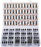
- Big Logic IC Assortment, 46 Types: CD4001, CD4011, CD4013, CD4015, CD4016, CD4017, C4021, CD4022, CD4023, CD4024, CD4025, CD4026, CD4027, CD4028, CD4029, CD4033, CD4042, CD4043, CD4046, CD4047, CD4049UBE, CD4050, CD4051, CD4052, CD4053, CD4060, CD4063, CD4066, CD4069, CD4070, CD4071, CD4072, CD4073, CD4075, CD4077, CD4081, CD4082, CD4093,CD4094, CD4503, CD4511, CD4518, CD4520, CD4541, CD4543, CD4553
- Every IC Type has 2 pcs, CD4017 and CD4049UBE are 4 pcs each
- Includes 10 pcs DIP-14 Sockets and 14 pcs DIP-16 Sockets
- Contains various usefull Logic ICs such as: NOR NAND OR AND Gates, Flip Flop, Shift Register, Bilateral Analog Switch, Decade Octal BCD Binary Counters, R/S Latch, Multivibrator, Hex Inverting Buffer, Multiplexer, Demultiplexer, Comparator, Exclusive Gate, Schmitt Trigger, Timer, PLL, 7-Segment Latch Decoder Driver, Frequency Divider
- Sorted accordingly in a labeled plastic box with pin configuration diagrams
Choose the version by the load sequence you need
- Use the CD4050B arrangement when the load should start off and turn on after the delay.
- Use the CD4049UB arrangement when the relay should start energized and then turn off after the delay.
- Check supply and relay coil voltage together. The project parts list pairs a 12 V supply with a 12 V relay; its 5 V note calls for a suitable 5 V relay.
- Consider reset behavior. The described circuit uses S1 to discharge C1 for quick reuse; the off-delay article also describes a modified reset/discharge path.
- Decide whether approximate timing is acceptable. These are RC threshold circuits, not precision or safety-critical timers.
Input and output limits to respect
TI lists a 3 V to 18 V operating range for these devices and applications including CMOS-to-DTL/TTL conversion, current driving, and high-to-low logic-level conversion. The datasheet discusses inputs above VCC in the context of logic-level conversion, but that is not a general permission to overdrive any pin. Its application procedure says CD4049UB inputs in the shown application must remain below VCC because of input clamp diodes.
- Keep inputs, outputs, and loads within the datasheet’s recommended conditions. In particular, TI says outputs should not be pulled above VCC and load current must remain within device power limits.
- Do not leave unused logic inputs floating; tie them to a defined logic level.
- Take care with slow RC input transitions. TI specifies recommended input rise/fall and logic-level conditions, while these timer examples rely on a gradual voltage rise; do not assume a slow transition is automatically within every recommended condition.
- Check the exact package and pinout for the part you have before wiring it.
Relay safety
The relay contacts may switch mains voltage even though the timing circuit uses a low-voltage supply. The project article calls for proper insulation, an enclosure, earthing, fuse protection, and adequate PCB spacing. Mains wiring presents a serious shock and fire risk; anyone without the required electrical experience should not build or handle a mains-connected version.
The Tool Desk
Outbyte PC Repair FREEClear out junk files and repair common Windows errorsFree Scan →Outbyte Driver Updater FREEScan for outdated or missing drivers - takes under a minuteDriver Scan →Quick Recap
Best Value

- Logic gate IC chip 10PCS CD4011 CD4001 CD4094 CD4060 CD4069 CD40106 CD4051 CD4052 CD4053 CD4093 CD4013 CD4017 SOP14 SOP16
Product prices and availability are accurate as of the date/time indicated and are subject to change. Any price and availability information displayed on Amazon at the time of purchase will apply.

