
Recommended Free Tools
Die stacking puts multiple bare silicon dies in one package; package stacking places already packaged chips on top of one another. Both can add silicon or memory capacity without using more board area, but they differ in yield, sourcing, package height, thermal behavior, and assembly complexity. The figures below come from David G. Morrison’s June 24, 2002 Electronic Design article, so they describe capabilities and expectations reported at that time—not 2026 specifications.
What is die stacking?
Die stacking, also called chip stacking, assembles multiple individual, unpackaged dies vertically inside a single package. A die may be stacked directly on another die or separated by a spacer when the lower die’s wirebonds need clearance. The package’s substrate and external connections then link the stack to the circuit board.

Because the dies sit close together, die stacking can reduce board footprint and shorten die-to-die signal paths. Shorter routes can reduce delay, inductance, and crosstalk. When a package combines several kinds of functional blocks, the broader design may be described as a system-in-package (SiP).
What is package stacking?
Package stacking vertically combines devices that have already been assembled into their own packages. Rather than handling bare dies in a shared enclosure, the manufacturer stacks known-good packaged components and connects them as an assembly. This can simplify the sourcing problem compared with bare-die stacking, although the added packages and interconnection materials increase height and material cost.
#1 Best Overall
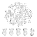
- [Multipurpose Use] - Plastic screws are mainly used in semiconductor manufacturing equipment, electronic manufacturing, food production lines, chemical equipment, automotive interior and exterior, DIY design, and other equipment that is sensitive to metal and rust-proof
- [Durable Screws and Nuts] - The material of the bolt and nut is acrylic, which has good weather resistance, excellent insulation, corrosion resistance and rust resistance, hard surface, wear resistance and long service life
- [Size & Package] - The size of the screw is 0.21 x 0.4 inches/5.5 x 10mm (Dia x L), the pitch is 0.5mm, and the nut size is 0.22 x 0.12 inches/5.5 x 3mm (L x H). The package contains 30 bolts and nuts
- [Advantage] - Transparent screws and nuts, with a delicate appearance without burrs, cross-slot disc screw holes, uniform installation force, clear and deep threads, not easy to slip, firmly tightened and beautiful
- [Attention] - Easy to install, just turn the cross screwdriver to complete the installation. Please confirm the required product size before purchasing
Both methods aim to fit more silicon or memory into a fixed board footprint and reduce the number of components mounted on the board. The choice depends on the application: die cost and count, availability of known-good die, allowable height, interconnect needs, heat dissipation, and the assembly process all affect which approach is practical.
How do die stacking and package stacking compare?
| Factor | Die stacking | Package stacking |
|---|---|---|
| What is stacked | Bare dies assembled together in one package. | Previously packaged devices stacked together. |
| Board footprint and signal paths | Can reduce board area and shorten die-to-die routes. | Can reduce the board area used by separate components, but adds package layers and connections. |
| Yield and sourcing | Yield depends on the dies in the stack; wafer-level known-good die (KGD) availability is important. | Uses known-good packaged devices, which can avoid combining untested bare dies in the final assembly. |
| Height and mechanics | Depends on die thickness, spacers, substrate, bond-wire loops, and external connections. | Has the height of the stacked packages plus the stacking interconnect and board connection. |
| Cost and process demands | Requires suitable bare-die supply and processes such as wafer thinning, thin-die attach, and low-loop wirebonding. | Adds package and stacking-material cost; assembly must withstand repeated solder reflow and possible rework. |
| Thermal behavior | Can make heat removal difficult when a high-power die is stacked with memory or another die. | Also constrains heat flow through a vertical assembly; the cited article does not quantify a thermal advantage for either method. |
The comparison is qualitative: Morrison’s article explains the trade-offs but does not give a controlled, like-for-like cost or thermal test for the two methods.
Why does known-good die matter?
In a die stack, every die contributes to the assembly’s yield. If any die is defective, the completed package may fail, so the practical yield depends on the yields of the dies being assembled. That makes wafer-level testing and access to known-good die important, especially as stacks contain more dies.
Assembly companies also need die in wafer form so the wafers can be thinned before singulation. A high-yield wafer or a wafer map identifying defective dies helps avoid spending assembly effort on known-bad parts. In the 2002 article, wafer-level KGD was described as obtainable for some lower-capacity NOR flash, while SDRAM, DSPs, and baseband processors were often difficult to source in that form.
Windows Errors? Fix Them Before They Spread
Repair common Windows errors and clear accumulated junk for a smoother, more stable PC - no reinstall needed.Free scan · no reinstallOutdated Drivers Are Slowing You Down
One free scan finds every outdated or missing driver and matches the right update for your exact hardware.Free scan · exact hardware matchPackage stacking starts with known-good packaged devices, which can reduce the risk associated with assembling several untested bare dies together. DPAC Technologies reported manufacturing yields above 97% for its package-stacking approach in 2002 and attributed them to using known-good packaged devices. That was the company’s reported result, not a general yield figure for package stacking.
How many dies or packages can be stacked?
There is no universal maximum in the 2002 article: feasible stack count depends on yield, component sourcing, package height, mechanical design, and thermal limits. As die count rises, the chance that a stack includes a defective die also rises, while sourcing KGD becomes harder.
Rank #3

- Sturdy And Construction: Made from high-quality bearing steel, this MGN15 linear motion component provides a stable structure for equipment requiring controlled movement. Its and low friction characteristics support consistent sliding performance, making it suitable for CNC parts, automation equipment, and other machinery where motion guidance is r
- Superior Stability For Precise Work: Designed for, low-friction movement, the guideway helps reduce during sliding and supports stable. The 15mm guideway width, 40mm guideway hole spacing, and 32 x 42.1mm slider size provide defined installation for users working on CNC equipment, 3D printers, semiconductor manufacturing equipment, and linear motio
- Lightweight And Portable Design: The compact MGN15 configuration is designed for small linear motion machinery and equipment where controlled movement is needed within a defined installation area. With a 15mm width and 350mm length, it can be into suitable mechanical assemblies, supporting practical installation for equipment builders, technicians,
- Essential Woodworking Carpenter Accessory: This component is intended for industrial and mechanical motion applications rather than general woodworking use. It can serve as a linear motion in suitable equipment, including printed circuit board systems, IC assembly equipment, and robotic arms where sliding and stable are required
- Versatile Application For Multiple Projects: Suitable for CNC parts, 3D printer parts, semiconductor manufacturing equipment, printed circuit boards, IC assembly equipment, robotic arms, and linear motion measurement equipment. The defined MGN15 specification helps users match the component with compatible automation and motion systems
For package stacking, DPAC reported devices containing as many as eight packages in 2002. More than 95% of its demand at the time was for two-chip stacks. These are historical company figures, not a statement of what a current product can support.
What limits wafer thinning and wirebonding?
Wafer thinning and handling
Thinning combines backgrinding with polishing to remove stress left by grinding. A very thin wafer cannot support itself reliably during handling, so it needs support on a membrane or frame. Morrison reported that this loss of self-support occurred at roughly 100 µm for 200-mm wafers and 150 µm for 300-mm wafers.
Do these 3 things before closing this tab:
1Repair Windows errors before they cause bigger problems2Fix the driver behind crashes, sound loss and screen glitches3Clear out junk files and repair common Windows errorsVendor capabilities reported in the 2002 article were approximately 100 µm for Amkor and ChipPAC on 200-mm wafers, 140 µm for ASE, and 150 µm for ChipPAC on 300-mm wafers. The article forecast 75–76 µm as the next capability and anticipated 50 µm on 300-mm wafers later; those were forecasts made in 2002, not current production limits.
Rank #4
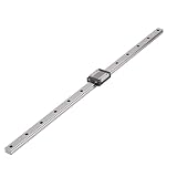
- Sturdy And Construction: Made from high-quality bearing steel, this MGN15 linear motion component provides a stable structure for equipment requiring controlled movement. Its and low friction characteristics support consistent sliding performance, making it suitable for CNC parts, automation equipment, and other machinery where motion guidance is r
- Superior Stability For Precise Work: Designed for, low-friction movement, the guideway helps reduce during sliding and supports stable. The 15mm guideway width, 40mm guideway hole spacing, and 32 x 42.1mm slider size provide defined installation for users working on CNC equipment, 3D printers, semiconductor manufacturing equipment, and linear motio
- Lightweight And Portable Design: The compact MGN15 configuration is designed for small linear motion machinery and equipment where controlled movement is needed within a defined installation area. With a 15mm width and 350mm length, it can be into suitable mechanical assemblies, supporting practical installation for equipment builders, technicians,
- Essential Woodworking Carpenter Accessory: This component is intended for industrial and mechanical motion applications rather than general woodworking use. It can serve as a linear motion in suitable equipment, including printed circuit board systems, IC assembly equipment, and robotic arms where sliding and stable are required
- Versatile Application For Multiple Projects: Suitable for CNC parts, 3D printer parts, semiconductor manufacturing equipment, printed circuit boards, IC assembly equipment, robotic arms, and linear motion measurement equipment. The defined MGN15 specification helps users match the component with compatible automation and motion systems
Die attach and wirebond clearance
Thin dies can be attached using dispensed paste epoxy or preformed tape epoxy. Wirebonded stacks may require loops below 100 µm, compared with roughly 150–175 µm for standard wirebonding, to keep the package thin. When dies are the same size, or a larger die sits over a smaller one, a silicon spacer can provide clearance for the lower die’s wirebonds.
Alternative interconnect approaches
Flip-chip-on-chip can connect dies pad-to-pad rather than relying on wire loops. The article also describes Valtronic’s repadding technique, which adds metallization and passivation so standard dies can be used in arrangements that might otherwise require a custom ASIC.
Independent reader supportYour contribution helps us test, update, and keep practical guides available for everyone.What determines package height?
Overall height is the sum of multiple layers, not just the silicon: substrate, die, spacer, interconnect loop, and external BGA balls all contribute. In its 2002 discussion, Morrison described two- or four-layer BT-core laminates, possible six-layer substrates, cores 80–100 µm thick, and thinner polyimide-tape substrates.
What’s actually slowing this PC down?
Pick the symptom - the matching free tool is one click away.
Best Value

- Sturdy And Construction: Made from high-quality bearing steel, this MGN15 linear motion component provides a stable structure for equipment requiring controlled movement. Its and low friction characteristics support consistent sliding performance, making it suitable for CNC parts, automation equipment, and other machinery where motion guidance is r
- Superior Stability For Precise Work: Designed for, low-friction movement, the guideway helps reduce during sliding and supports stable. The 15mm guideway width, 40mm guideway hole spacing, and 32 x 42.1mm slider size provide defined installation for users working on CNC equipment, 3D printers, semiconductor manufacturing equipment, and linear motio
- Lightweight And Portable Design: The compact MGN15 configuration is designed for small linear motion machinery and equipment where controlled movement is needed within a defined installation area. With a 15mm width and 350mm length, it can be into suitable mechanical assemblies, supporting practical installation for equipment builders, technicians,
- Essential Woodworking Carpenter Accessory: This component is intended for industrial and mechanical motion applications rather than general woodworking use. It can serve as a linear motion in suitable equipment, including printed circuit board systems, IC assembly equipment, and robotic arms where sliding and stable are required
- Versatile Application For Multiple Projects: Suitable for CNC parts, 3D printer parts, semiconductor manufacturing equipment, printed circuit boards, IC assembly equipment, robotic arms, and linear motion measurement equipment. The defined MGN15 specification helps users match the component with compatible automation and motion systems
BGA ball size and pitch also set a lower bound on package height. The article cited ball diameters ranging from 0.75 mm at 1.27-mm pitch to 0.2 mm at 0.35-mm pitch. These dimensions are historical examples from 2002, not a current catalog of package options.
For portable products, the article reported demand moving toward package heights of 1.2 mm and 1.0 mm, with 0.8 mm considered a possible target. It also described three- and four-die stacks in 1.4-mm packages. Those reports capture the market and capabilities described at the time.
How do yield, cost, and thermal limits change the choice?
Yield and cost as stacks grow
More dies increase the number of parts that must be good and the difficulty of obtaining KGD. Package stacking adds package and interconnect material, but using known-good packaged components can make yield more predictable. Morrison’s 2002 analysis therefore presented package stacking as increasingly attractive as die count and die cost rose, while emphasizing that the application determines the better option.
Heat removal
Stacking can make it harder for heat to escape, particularly when a high-power processor shares a vertical package with memory. The article noted that graphics processors dissipating 3 W or more required heatsinking, complicating processor-memory stacks. This is a specific historical example, not a universal power threshold for present-day designs.
Assembly and reliability demands
Package-stacking materials must tolerate multiple surface-mount reflow cycles and rework. Morrison reported that early production work focused on thin, flat, high-temperature, moisture-resistant leadframe packages such as TSOPs, while CSP and BGA stacking were still under development in the context of the article.
What did a footprint reduction look like?
As a 2002 example, Advanced Semiconductor Engineering (ASE) compared a Mini-PC card with separate 2.4-GHz RF, logic, and DSP chips against a stacked-die multichip BGA design. ASE reported that the stacked design occupied 729 mm², versus 3,225 mm² for the separate-chip arrangement. This is the area comparison reported for that specific example; it is not a general reduction ratio for all stacked packages.
Quick Recap
Product prices and availability are accurate as of the date/time indicated and are subject to change. Any price and availability information displayed on Amazon at the time of purchase will apply.

