
For a square wave, an adjustable phase shift is normally a controlled time delay. Set the delay to td=φ/(360°f); covering 0° to 180° therefore requires 0 to T/2=1/(2f). A practical digital signal path is Schmitt-trigger buffer → variable or programmable delay → Schmitt-trigger buffer. Use a PLL/DLL or a timer that measures the period when frequency changes. Use only an inverter when the requirement is a fixed 180° complement.
Convert the phase requirement to time first
Phase is relative to frequency, while a delay is measured in seconds. For a periodic input frequency f and requested phase φ:
td=φ/(360°f)
For the full 0°–180° range, the hardware must provide:
0≤td≤T/2=1/(2f)
| Input frequency | Period | Delay for 180° |
|---|---|---|
| 1 kHz | 1 ms | 500 µs |
| 10 kHz | 100 µs | 50 µs |
| 100 kHz | 10 µs | 5 µs |
| 1 MHz | 1 µs | 500 ns |
| 10 MHz | 100 ns | 50 ns |
A fixed 500 ns delay is 180° at 1 MHz, 360° at 2 MHz, and 90° at 500 kHz. It is a fixed time offset, not a fixed phase, unless the frequency is fixed.
#1 Best Overall

- Working voltage: 5V
- Working current: <50mA
- Input voltage range: +/-0.1V~+/-5V
- Output voltage range: 5V
- Input frequency: 50Hz~60MHz
Decide what “180°” means
Delayed copy
A half-period delay moves every edge by T/2 and preserves the waveform’s duty cycle. This is the usual meaning of a phase-shifted copy.
Logical complement
An inverter exchanges the high and low states. For an ideal periodic 50% duty-cycle square wave, that is the logical equivalent of 180° for the fundamental, but it is not an adjustable 0°–180° circuit. An inverter also has propagation delay.
Analog phase rotation
An all-pass filter changes the phase of each frequency component. A square wave contains a fundamental and harmonics, so those components receive different phase shifts and the edges are distorted. A first-order stage has H(s)=(1−sRC)/(1+sRC) and φ(f)=−2tan−1(2πfRC); its phase is frequency-dependent, even though its ideal magnitude is constant. See TI’s active-filter note at https://www.ti.com/lit/pdf/sloa088.
Rank #2

- High-precision low-frequency phase module
- Adding first-stage phase amplification on the basis of the original one
- Can achieve signal phase within 500KHz
- Phase range: 0°~360°(default 1KHz low frequency)
- For high-frequency phase it needs to be replaced with corresponding capacitors
Best circuits for a clean square-wave output
1. Programmable digital delay line
For a fixed or slowly changing frequency, use a logic buffer, a selectable delay, and an output buffer:
input square wave → Schmitt buffer → programmable delay → Schmitt buffer → output
The delay code can be parallel- or serial-programmed and latched before it affects the signal. Analog Devices describes this operating mode, enable/latching behavior, and pulse-width constraints for the DS1020/DS1021 family at https://www.analog.com/en/resources/technical-articles/ds1020ds1021-8bit-programmable-delay-lines.html.
With N equally spaced codes spanning 0°–180°:
Δt=(T/2)/(N−1) and Δφ=180°/(N−1).
- Real parts have nonzero minimum propagation delay; code zero is rarely zero delay.
- Delay accuracy and edge-to-edge skew vary with supply, temperature, process, loading, and input slew rate.
- Rising and falling edges may not have identical delay, producing duty-cycle error.
- The selected delay must fit the usable pulse width and period. A delay comparable to a pulse width can create unexpected edge relationships.
- Legacy parts may be difficult to source or incompatible with modern logic voltages. Verify lifecycle, voltage range, timing, and stock before designing around them.
Delay-line architecture and compensation for process, voltage, and temperature variation are discussed at https://www.analog.com/en/resources/technical-articles/how-delay-lines-work.html. A dual 4-bit example, including discrete steps and pulse-width considerations, is documented at https://www.analog.com/en/resources/app-notes/device-characteristics-of-the-ds1045-dual-4bit-programmable-delay-line.html.
Rank #3
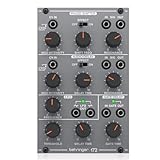
- amazing phase shifter/delay/lfo module from the '80s
- "authentic reproduction of original ""system 100m"" circuitry"
- 6-step phase shifter with mod intensity, shift frequency and resonance controls
- analog bbd delay with mod intensity, delay time and resonance controls
- gate delay with threshold, delay time and gate time controls for creative pulse shaping
2. Hardware timer or output-compare peripheral
At low or moderate frequencies, a microcontroller can track the period and schedule the output in hardware:
- Capture an input edge with a timer.
- Measure the period
T. - Calculate
td=(φ/360°)T. - Program an output-compare event for that delay.
- Toggle or set the output at the scheduled event.
- Recalculate when the measured frequency changes, and define timeout behavior if the input stops.
Use capture/compare hardware, not ordinary interrupt-driven GPIO. Interrupt latency, timer quantization, metastability at an asynchronous input, input jitter, and an abnormal pulse after a sudden frequency change are common failure modes. For power switching, firmware must not be the only shoot-through protection.
Quick wins for a faster PC:
Clear out junk files and repair common Windows errorsFree Scan →Fix the driver behind crashes, sound loss and screen glitchesFind Drivers →3. FPGA or clock IC PLL/DLL
For a clock, high frequency, multiple outputs, or phase that must track frequency, feed the signal into a dedicated clock input and use a PLL, DLL, or clock-management block. Generate a reference output and a programmable 0°–180° output on dedicated clock resources:
Rank #4

- 2pcs MCP41010 Circuit Precision Programmable Phase Shifting Amplifier Adjustable 0-360 Degree Variable Phase Shifter Circuit Module Board
input clock → clock input → PLL/DLL → 0° output and programmable phase output
Phase range, step size, lock time, jitter, VCO limits, divider settings, and output skew are device-specific. Microchip documents PLL/DLL phase shifting and digitally controlled I/O delays in its PolarFire SoC overview: https://ww1.microchip.com/downloads/aemDocuments/documents/FPGA/ProductDocuments/ProductBrief/PolarFire-SoC-Product-Overview-60001656.pdf. Do not assume a universal resolution or route a clock through ordinary fabric logic when dedicated resources are available.
4. Fixed inverter
If only a complement is required, use a logic inverter or Schmitt inverter. It is the lowest-component-count solution, but it offers no adjustment and does not create programmable dead time.
5. Analog all-pass plus comparator
An RC/op-amp all-pass network can provide continuously adjustable phase around a selected frequency. A digital potentiometer can control such a network; an example is described at https://www.analog.com/en/resources/app-notes/digitallycontrolled-phase-shift-using-the-ds1669.html. To recover logic, follow it with a comparator or Schmitt trigger. The switching point then depends on frequency, duty cycle, amplitude, slew rate, threshold, hysteresis, resistor and capacitor tolerances, and comparator delay. This is suitable for narrow-band experiments, not a general broadband square-wave clock.
Free tools Windows power users keep installed
One-click scans. No signup required.
Best Value
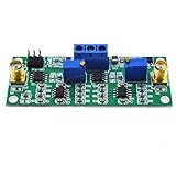
- MCP41010 Circuit Precision Programmable Phase Shifting Amplifier 0-360 Degree Variable Phase Shifter Circuit Module Board
Worked phase-resolution examples
1 kHz timer-controlled signal
At 1 kHz, T=1 ms and the 180° endpoint is 500 µs. A timer clocked at 1 MHz has 1 µs ticks, giving approximately 0.36° per tick. Capture the input period and calculate the compare offset from the measured period so the phase remains proportional if the frequency drifts.
1 MHz programmable delay
At 1 MHz, the required range is 0–500 ns. One degree equals 1 µs/360=2.78 ns; 0.1° equals 278 ps. A delay device with only a few-nanosecond step size cannot honestly provide 0.1° resolution, regardless of its nominal phase-control label.
High-speed clock
Use the selected FPGA or clock IC’s phase-shift primitive, verify its legal input and VCO ranges, and include lock time and jitter in the system startup sequence. Measure phase at the actual receiving pins, not only at an internal simulation node.
Duty cycle, jitter, and waveform integrity
- A delayed copy preserves duty cycle; inversion swaps high and low intervals. For non-50% duty cycles these are not interchangeable.
- Phase error from timing error is
Δφ=360°fΔt. The same 1 ns error is negligible at 1 kHz but 36° at 100 MHz. - Slow edges make threshold-dependent phase measurements noisy. Restore logic levels with a suitable Schmitt trigger or buffer.
- Check input/output voltage standards, capacitive load, rise and fall times, transmission-line termination, and buffer propagation delay.
- Changing a delay code while an edge is propagating can produce runt or missing pulses. Latch settings synchronously, update during a safe window, or use glitchless clock-control resources.
Power-electronics warning
A phase-shifted logic waveform is not automatically safe gate drive. An inverter can turn one switch on before the other has fully turned off because of unequal propagation delays, MOSFET storage, Miller effects, and driver turn-off delay. Use a half-bridge or full-bridge driver with hardware interlock and specified dead time. Verify both gate-source voltages with an appropriate differential probe across temperature, load, and supply extremes. A phase shifter does not provide isolation, current drive, fault protection, or dead time by itself.
Crashes, No Sound, or Screen Glitches?
Random freezes, missing sound and display glitches usually trace back to one bad driver. Find and replace yours safely.Free scan · under a minuteWindows Errors? Fix Them Before They Spread
Repair common Windows errors and clear accumulated junk for a smoother, more stable PC - no reinstall needed.Free scan · no reinstallMeasurement and commissioning
- Probe input and output with matched, bandwidth-appropriate probes and a common voltage reference.
- Measure rising-edge-to-rising-edge and falling-edge-to-falling-edge delay separately.
- Record duty cycle, overshoot, ringing, and jitter over many cycles.
- Check minimum, midpoint, and maximum delay codes, including the actual minimum propagation delay.
- Repeat measurements at every operating frequency, supply voltage, temperature, and load that matters.
- Change the control code during operation and confirm that no runt pulses or unsafe overlap occur.
Selection checklist
- Input frequency range and whether it is fixed or variable.
- Required phase range, step size, absolute timing accuracy, and jitter.
- Logic voltage, signal standard, duty cycle, edge-rate limits, and load.
- Continuous versus stepped control and analog versus digital adjustment.
- Whether inversion is acceptable and whether the output drives a clock, logic input, or power transistor gate.
- Startup, loss-of-input, reconfiguration, interlock, and fault behavior.
| Requirement | Preferred architecture |
|---|---|
| Exactly 180° only | Logic inverter or complementary output |
| Fixed frequency, selectable delay | Programmable delay line |
| Variable frequency with tracked phase | PLL/DLL, FPGA clock block, or timer-based proportional delay |
| Low-frequency experiment | Hardware timer or RC/comparator |
| High-speed clock | Dedicated PLL, DLL, or calibrated delay resource |
| Power switching | Gate driver with dead time and interlock |
The Bottom Line
For a clean adjustable square wave, design in time first: provide 0 to T/2 delay, then restore the logic level. Choose a programmable delay for a fixed frequency, a timer or PLL/DLL when frequency varies, and an inverter only for a fixed complement. Keep waveform integrity, code-update glitches, jitter, and power-stage dead time separate from the phase-shift function.
Quick Recap
Product prices and availability are accurate as of the date/time indicated and are subject to change. Any price and availability information displayed on Amazon at the time of purchase will apply.

