
For glitch-free clock switching, use a clock-specific mux or switching primitive supported by the target device—not an ordinary logic mux—and follow its documented control timing and clock-activity requirements. The safe choice depends on whether the inputs are related or independent, whether both clocks remain active during handoff, and how much switching delay the design can tolerate.
Why an ordinary mux can glitch
A clock drives state changes in sequential logic, so an unintended edge or shortened pulse can trigger logic at the wrong time. A plain combinational mux can change its output as soon as its select input changes. If its clock inputs are at different logic levels, that change may create a malformed pulse. A data mux is therefore not automatically safe to use on a clock path.
Clock-specific switching structures control when the new clock is allowed through. Altera’s clock-multiplexing guidance describes a structure that enables a new clock only after the other clock is inactive. In the example described, the outgoing clock must continue for at least a few cycles; stopping it immediately can prevent the handoff from completing.
Choose a switching method for the target hardware
There is no universal glitch-free mux circuit with the same guarantees across FPGA families and external clock devices. Start with the exact part’s clocking resources and documentation, then check the conditions that apply to your clock relationship and control signals.
Do these 3 things before closing this tab:
1Scan for outdated or missing drivers - takes under a minute2Repair Windows errors before they cause bigger problems3Fix the driver behind crashes, sound loss and screen glitches#1 Best Overall

- Wide Range of Digital Levels:Digital 3V to 20V
- Low ON Resistance, 125Ω (Typ) Over 15VP-P Signal Input Range for VDD-VEE = 18V
- High OFF Resistance, Channel Leakage of ±100pA (Typ) at VDD-VEE = 18V
- Binary Address Decoding on Chip
- 100% Tested for Quiescent Current at 20V
| Option | Documented use and conditions | Handoff timing |
|---|---|---|
| AMD Versal BUFGCTRL | AMD describes it as a synchronous/asynchronous glitch-free 2:1 mux. CE0 and CE1 have setup/hold requirements; violating them could cause a clock glitch. See AMD BUFGCTRL documentation. | Not stated in the cited documentation summary; consult the exact device documentation. |
Altera ipm_cdc_glitchless_clk_mux |
Supports related or unrelated clocks according to the CLK_TYPE setting. Misclassifying unrelated clocks as related may cause a glitch. Both clocks must be toggling before and after the select change for switching to complete. See Altera macro documentation. |
For related clocks, the macro waits for the next falling edge of each clock; for unrelated clocks, it waits for the second falling edge of each. |
| Microchip PolarFire NGMUX | Supports dynamic glitch-free switching between independent clocks. The published behavior is specific to PolarFire. See Microchip PolarFire documentation. | With both clocks active, Mode 0 is documented to take up to three current-clock cycles plus three new-clock cycles. Mode 1, for a current clock that is inactive or uncertain, is documented to take up to 50 new-clock cycles with a minimal chance of glitch. |
| Renesas 580-01 external clock mux | Renesas describes the part as switching between two clock sources without glitches or short pulses. Verify electrical compatibility and detailed timing in the current product datasheet. See Renesas 580-01 product page. | Consult the current datasheet for the exact timing. |
Design checks before switching
- Identify the exact device. Confirm the FPGA family or clock-mux IC and use its supported clocking resource. A primitive from another family may not have the same placement, behavior, or guarantees.
- Classify the clock relationship. Determine whether the sources are related or unrelated according to the vendor’s definition. For the Altera macro, set
CLK_TYPEaccordingly; configuring related clocks when the sources are unrelated may allow a glitch. - Check enable and select timing. Follow the setup/hold requirements for each control pin. AMD explicitly warns that failure to meet BUFGCTRL’s CE timing requirement could result in a clock glitch.
- Keep clocks active when required. The Altera macro requires both clocks to toggle before and after a select change. The generic Altera structure also needs the outgoing clock to continue for at least a few cycles in the described example. Do not assume a handoff will complete if a source stops at the request.
- Allow for the handoff interval. A glitch-free transition is not necessarily immediate. Determine the applicable worst-case timing for the selected primitive and mode, and ensure the surrounding system can tolerate the resulting clock pause or transition interval.
- Review reset and CDC behavior separately. A source or frequency change can affect reset sequencing and clock-domain crossings, but the cited vendor material does not establish one reset or CDC recipe that applies to every design.
Can you switch between unrelated clocks?
Some device-specific solutions explicitly support independent clocks, but that does not make every clock mux safe for arbitrary inputs. Microchip documents PolarFire NGMUX for independent clocks, while Altera’s parameterized macro supports related and unrelated clocks only when configured for the correct relationship. AMD BUFGCTRL’s documented control requirements must also be met. Check the exact primitive’s support and timing rather than inferring behavior from another family’s implementation.
What if one clock stops during the handoff?
Stopped-clock behavior is primitive-specific. Altera’s macro requires both inputs to be toggling before and after the select change, so a stopped source can prevent switching from completing. PolarFire NGMUX documents a separate Mode 1 for cases where the current clock is inactive or uncertain, with a stated bound of up to 50 new-clock cycles and a minimal chance of glitch. That Mode 1 behavior is a PolarFire-specific guarantee, not a general property of clock muxes.
Rank #2

- Comprehensive IC Assortment: This kit includes a carefully selected combination of 74HC series and 74LS series logic ICs, featuring 22 types with 55 total pieces including IC sockets to meet your basic maintenance needs for daily electrical appliances and projects
- Complete Model Selection: Includes 74LS00, 74LS02, 74LS04, 74LS08, 74LS32, 74LS47, 74LS74, 74LS86, 74LS90, 74LS138, 74LS164, 74LS245, 74HC00, 74HC02, 74HC04, 74HC08, 74HC14, 74HC32, 74HC138, 74HC164, 74HC165, and 74HC595 with two of each type, plus DIP14, DIP16, and DIP20 sockets
- Integrated Circuit Advantages: Features small size, light weight, minimal solder joints, long lifespan, high reliability, and good performance characteristics that increase assembly density by hundreds of times compared to transistors while improving equipment stability
- Versatile IC Types Included: Contains various useful IC types for daily maintenance and assembly including shift output registers, transceivers, decade counters, multiplexers, decoders, and hex inverters for diverse electronic applications
- Wide Application Range: Low power consumption with strong processing capability, suitable for various terminal industries including industrial control products, automotive electronics, medical equipment, security monitoring, household appliances, laboratory work, and communication equipment
How to choose between FPGA logic and an external mux IC
For an FPGA design, first evaluate the target family’s dedicated clock-switching resources: their placement, supported clock relationships, control timing, activity requirements, and handoff delay. An external clock mux IC may suit a board-level source switch, but verify the part’s electrical interface, supported frequencies, and detailed timing against the system requirements. The Renesas 580-01 is one documented example; its product description alone is not enough to establish suitability for a particular circuit.
Quick Recap
Best Value

- 1, 【 What You Get 】 ----- In this kit, We carefully select the combination of 74HCXX series and 74LSXX series for you to meet your needs for IC chip work. 21 type, 2Pcs each type In total 44Pcs,and 5pcs IC Socket. So Many different Types popular IC Chip can meet all your Daily needs.
- 2, 【 Detailed List 】 ----- 74LS00,74LS02,74LS04,74LS08,74LS32,74LS47,74LS74,74LS86,74LS90,74LS138,74LS164,74LS245, 74HC00, 74HC02, 74HC04 ,74HC08,74HC14,74HC32,74HC138,74HC164,74HC165,74HC595. 2 pcs DIP14 socket, 2 pcs DIP16 socket,1 pcs DIP20 socket.
- 3, 【 Product Features】 -----Integrated circuits have the advantages of small size, light weight, small solder joints, long life, high reliability, and good performance. At the same time, the cost is low and it is convenient for mass production. Using integrated circuits to assemble electronic equipment, the assembly density can be increased by tens to thousands of times than that of transistors. The stable working time of the equipment can also be greatly improved.
- 4,【 The Most Popular 74LSx Series IC Chip Kit】 ------ We have chosen a variety of useful IC types for daily assembly, such as: Photocouplers, Timers, Osciallators, Dual Opamps, Quad Opamps, Comperators, Audio Amplifiers, Echo Processors, Current Mode Controllers, Darlington Arrays, Voltage Charge Pump, etc.
- 5, 【 Wide Applications】----- low power consumption, strong anti-interference, small and flexible, strong processing capacity, green and environmental protection, suitable for most terminal industries, such as industrial control products, automotive electronics, medical equipment, security monitoring, household Electrical appliances, student experiments and communication equipment.
Rank #4
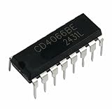
- Package Contents and Type: Pack of 10 Pcs in DIP-16 Package format
- Logic Function: Quad Bilateral Analog Switch for versatile signal routing applications
- Voltage Range: Wide operating voltage range from 3V to 18V for flexible power supply options
- Low On-Resistance: Ultra-low RON of 50 ohms typical at 15V for minimal signal degradation
- Independent Switching: Features four independent switches for transmission or multiplexing of analog or digital signals
Rank #3

- SN74LS157N is a quad 2-input multiplexer with common select using low-power Schottky technology
- Data selection in TTL systems multiplexing applications and data routing requiring quad capability
- Good noise immunity with common select input and strobe control for reliable operation
- Quad 2-input multiplexers with common select and strobe input for TTL systems
- TTL data selection multiplexer systems and data routing applications
Product prices and availability are accurate as of the date/time indicated and are subject to change. Any price and availability information displayed on Amazon at the time of purchase will apply.

