
A zero-delay clock buffer uses feedback to align a clock edge at a chosen output or receiver with a reference edge. It does not eliminate the signal’s physical travel time: the PLL or DLL adjusts phase or delay so that the returned edge matches the reference at the defined alignment point.
What “zero delay” means in a clock system
In a zero-delay arrangement, a phase detector compares the reference clock with a copy of the clock returned from a point in the output path. That point might be after an output driver, a fanout buffer, a PCB trace, or another part of the target path. The control loop adjusts clock phase or delay until the returned edge aligns with the reference.
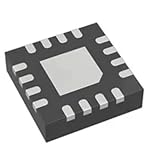


Microchip describes a zero-delay buffer as producing a phase-aligned copy of the input at its output pins, for distributing one clock to multiple external components with low skew. Its guidance calls for external-feedback PLL operation and matching the routing delay from CLK_OUT to the external component with the routing delay from CLK_OUT to the PLL feedback clock.
Analog Devices explains the timing idea in terms of two points: when the variable delay equals the output driver’s propagation delay plus the interconnect delay, the clock edge at the target point can coincide with the reference edge. This is zero delay in relative timing, not zero elapsed time for a signal to propagate.
Free tools Windows power users keep installed
One-click scans. No signup required.
How external feedback compensates the output path
With external feedback, the clock output travels through the path whose delay matters, and a returned copy enters the PLL’s feedback input. Because the loop observes that path, it can compensate for its insertion delay. The relevant alignment is at the feedback observation point; any path after that point is not automatically corrected.
- Choose the alignment planes. Decide whether the required edge relationship is at an FPGA register, connector pin, fanout output, or remote receiver. The feedback path must represent the path to that plane.
- Route the clock through the representative path. Include the same output driver, package, connector, and representative PCB routing that the clock will use to reach the target.
- Use the device’s intended feedback resources. Connect the returned clock to the PLL feedback input and output pins or other dedicated resources required by the vendor. Do not substitute fabric routing where the device guidance requires dedicated clock resources.
- Match the compared paths. Keep output and feedback routing, loading, and relevant driver characteristics as similar as the design requires. In Microchip’s implementation guidance, the routing delays from CLK_OUT to the external component and from CLK_OUT to the PLL feedback clock should match.
- Configure the clock relationship. Set multiplication or division and any phase controls for the desired output frequency and edge relationship. Check that the selected output and feedback paths use compatible settings.
- Verify operating margins. Check lock range, jitter, duty cycle, setup and hold requirements, and process, voltage, and temperature limits for the actual device and design.
The loop corrects the delay it can observe. If the target’s path differs from the feedback path—for example, because of unequal trace length, load, divider settings, or receiver behavior—a residual skew can remain.
PLL and DLL: which mechanism fits?
A PLL and a DLL can both align clock edges using feedback, but they do not provide the same functions. A PLL can synthesize a frequency related to its reference as well as adjust phase. A DLL primarily changes a delay-chain setting to align edges; it is useful when delay or phase adjustment is needed without a separate oscillator.
| Design question | PLL | DLL |
|---|---|---|
| Frequency translation | Can multiply or divide the reference frequency, subject to the device’s supported settings. | Primarily tunes delay and phase; frequency translation is not established here as a general DLL capability. |
| How alignment is adjusted | Adjusts the PLL’s phase or frequency through feedback. | Adjusts a delay chain until the feedback and reference edges align. |
| Including a remote target path | External feedback can include the output path in the loop. | Feedback can align the paths implemented by a particular design, but the available information does not establish a general remote-path capability across DLLs; check the device’s implementation guidance. |
| Typical fit | Use when frequency synthesis and deskew are both required. | Use for insertion-delay removal, phase-shift generation, or duty-cycle correction when a separate oscillator is unnecessary. |
| Lock behavior, jitter, phase range, and power | Device-specific; not stated as a general comparison here. | Device-specific; not stated as a general comparison here. |
These are functional distinctions, not a claim that every PLL or DLL supports external clock deskew. Confirm the device’s supported modes, pins, and operating limits before choosing a topology.
Internal feedback, external feedback, and ZDB modes
Internal or normal feedback is generally used to optimize timing within a device’s internal clock network or register paths. It does not compensate a remote board path unless that path is actually included in the feedback loop. External feedback instead returns a clock from the selected output path so the loop can account for its delay.
Altera’s mode descriptions distinguish external feedback, which compensates the fbclk path, from zero-delay-buffer (ZDB) operation, which confines feedback to the dedicated external output and phase-aligns the off-chip clock with the input. In Stratix 10 ZDB, a bidirectional I/O pin mimics output-path delay. Altera’s guidance requires matching single-ended I/O standards and advises against board traces on that feedback pin because they can cause reflections.
| Topology | What the loop observes | Practical implication |
|---|---|---|
| Internal or normal feedback | The internal clock path represented by the device’s feedback configuration. | Useful for internal clocking goals, but a remote board path is not corrected unless routed into feedback. |
| External feedback | The returned clock path, including external routing or components placed before the observation point. | Can compensate the selected output path; requires suitable feedback pins and careful board routing. |
| Device-specific ZDB | The dedicated external-output path, as defined by that device’s mode. | Pin, I/O-standard, and routing rules can be restrictive. Follow the device guidance rather than assuming all output paths are included. |
Why aligned outputs can still have skew or propagation delay
Feedback can align edges only at its defined reference and target planes. It cannot remove the time a signal takes to travel, nor can one feedback observation guarantee that every output and receiver sees an identical edge.
- Unequal interconnects: Different trace lengths, connectors, loads, or output drivers create different path delays. Analog Devices identifies unequal external interconnects and internal channel skew as practical sources of residual skew.
- Channel and divider mismatches: Outputs that use different divider or delay settings may not have matching edge timing. Treat channels used for zero-delay distribution equivalently, including their divider and delay settings.
- Feedback-path noise: Periodic noise coupled into the feedback net can affect the loop and corrupt output timing. Keep the feedback net short and shielded, and avoid injecting noise into it.
- Loop stability: External delay is part of the loop. Excessive delay can destabilize a PLL if loop bandwidth and filter components are not selected for that delay.
- Device-specific constraints: FPGA ZDB modes may impose I/O-standard restrictions or special bidirectional-pin rules, and unsuitable board routing can introduce reflections.
Device figures are not universal design limits
An Analog Devices note from 2006 reports that the AD9520/AD9522 provide approximately 1100 ps of programmable delay range in approximately 120 ps steps, along with example channel-skew values. These are characteristics reported for those specific devices, not general limits for PLLs, DLLs, or zero-delay clock systems. The same material identifies the AD9520 as an integrated example combining a PLL, programmable delay, and twelve output drivers; verify the current device documentation for the exact configuration and specifications relevant to a design.
Recommended Free Tools
Quick Recap
Best Value

- 1 Pcs Clock Generator/Frequency Synthesizer/PLL AD9512BCPZ-REEL7 1.2 GHz Clock Distribution IC, 1.6 GHz Input, Divider, Delay Adjust, Five Outputs LFCSP-48(7x7)
Product prices and availability are accurate as of the date/time indicated and are subject to change. Any price and availability information displayed on Amazon at the time of purchase will apply.

