
Recommended Free Tools
iTechGuides is reader-supported. When you buy through links on our site, we may earn an affiliate commission. As an Amazon Associate I earn from qualifying purchases. Learn more
In March 2005, Intel and Texas Instruments were pushing toward 65-nanometer chip manufacturing while much of the semiconductor industry was still moving into 90 nm. Their head start reflected different business priorities: Intel was preparing smaller, lower-power multicore processors, while TI aimed to pack more wireless and signal-processing functions into handset chips. The 65 nm node promised more transistors per die, but it also brought higher wafer costs and fresh power, design, and manufacturing challenges.
What the 65 nm move meant in 2005
A process node describes a generation of semiconductor manufacturing technology. Moving from 90 nm to 65 nm was intended to let manufacturers fit more transistors into a given area and improve the economics or performance of particular chip designs. It did not mean every 65 nm chip would automatically run faster or use less power: those outcomes depended on the design and process choices.
EE Times reported on March 7, 2005, that Intel Corp. and Texas Instruments Inc. appeared to be a full process generation ahead of much of the industry. That was a statement about their development and production plans at that time, not a claim about current manufacturing leadership. EE Times report
Free tools Windows power users keep installed
One-click scans. No signup required.
Why Intel and TI were moving early
TI: more handset functions on a chip
TI said it had delivered “fully functional” samples of a 65 nm wireless-baseband device. Nokia was presumed to be the customer in the report, rather than confirmed by the cited statement. Analyst Will Strauss expected TI to ship 65 nm cellphone chipsets late in 2005. The proposed benefit was room for greater integration of functions such as Bluetooth, PDA features, high-resolution cameras, GPS, and Wi-Fi in a handset.
#1 Best Overall

- Diameter: 8 inches (203mm)
- Unique Iridescent Wafer Light Effect - The wafer has premium optical refractive properties that transform into different hues with different light and angles. The dynamic iridescent glow delivers a futuristic tech aesthetic, making it a unique, eye-catching addition to any space.
- Dual-Purpose Display Decoration - Comes with a free matching display stand that can be placed on a table or shelf. It can also be hung on the wall as a minimalist piece of technological art, perfectly matching the decor of your home, study, and office.
- High-End Black Gift Box Packaging - Equipped with a high-end black gift box, no additional packaging is required, very suitable for personal collection and exquisite gift giving
- MULTI-FUNCTIONAL GIFT AND DECORATION - Featuring a stylish, one-of-a-kind design, this wafer ornament is the perfect everyday decoration or a thoughtful gift for tech enthusiasts and friends.
TI planned three process variants to serve distinct designs: a low-voltage version for cellphone ICs, a general-purpose version for digital signal processors (DSPs), and a high-performance version for Sun Microsystems UltraSPARC designs. Those variations illustrate why a node was not a single uniform recipe; manufacturers tuned process characteristics to different power and performance needs.
Intel: multicore and power management
Intel discussed Yonah, a dual-core 65 nm processor expected at the end of 2005, and projected that as many as six 65 nm microprocessors would enter production in 2006. The strategic shift was away from relying only on higher clock speeds and toward multicore designs and power-management methods for desktop and server processors.
Rank #2

- Durable polypropylene construction ensures maximum protection for your wafers during handling and storage.
- devised for cleanroom environments, these cases meet Class 100 standards, making them ideal for semiconductor and electronics applications.
- Pack of 10 provides excellent value and convenience for laboratories and manufacturing facilities requiring multiple carriers.
- Each case securely holds a single wafer, preventing damage and while maintaining optimal cleanliness.
- Lightweight and easy to stack, these wafer cases are perfect for efficient storage and transportation in high-tech environments.
Mercury Research analyst Dean McCarron said the process was a likely route to 5 GHz, but he also pointed to Intel’s move toward multicore, multithreading, and power management. That was a contemporary assessment of the technology’s potential and direction—not evidence that a specific 65 nm Intel processor reached 5 GHz.
What 65 nm could improve—and what it cost
TI executive Dennis Buss said the added process complexity increased wafer cost by 20 percent while lowering cost per die by 40 percent. These were TI’s 2005 figures, not an industry-wide guarantee. The distinction matters: each wafer could cost more to manufacture, yet yield more or smaller dies, potentially improving unit economics for high-volume products.
Rank #3

- IC Type: Semiconductor
- Each wafer fragment contains visible integrated circuit patterns for demonstration and display purposes only.
- Made from single-crystal silicon wafer material for authentic semiconductor teaching and research.
- Ideal for electronics courses, microfabrication demonstrations, and STEM student projects.
- Also suitable for art installations, photography props, and chip design exhibitions.
Buss also described possible performance gains from silicon engineering: 10–15 percent from oriented silicon and up to 25 percent from deposited silicon-germanium (SiGe) strain. These were potential gains cited by TI in 2005, not independently established results for every 65 nm product. The actual benefit depended on implementation and the rest of the chip design.
Power and manufacturing challenges
More transistors also meant more power-management work
TI described dynamic voltage scaling, SRAM back-biasing, and retention flip-flops as techniques to reduce power. Such methods let a design adjust operating conditions or retain needed state while limiting energy use. The report’s broader warning was that 65 nm might repeat the difficulties seen at 90 nm, where leakage and power dissipation drove adoption of multiple threshold voltages, voltage islands, and dynamic voltage/frequency adjustment.
Rank #4
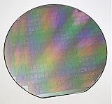
- - Diameter: 6 inches/Material: High-purity silicon
- - Type: Semiconductor integrated circuit substrate (4AD1 type)
- - Surface Finish: Polished for optimal film deposition
- - Thickness: Standard wafer thickness for IC applications
- - Application: Suitable for various integrated circuit designs and semiconductor devices
Strain, crystal orientation, and interconnects
The performance discussion included strained silicon, alternative crystal orientations, and SiGe strain in source/drain regions. These approaches sought to improve transistor behavior, but process gains had to be balanced against complexity and design constraints. Keeping interconnects short also mattered: faster or denser transistors cannot eliminate delays and power costs associated with signals traveling across a chip.
Do these 3 things before closing this tab:
1Repair Windows errors before they cause bigger problems2Fix the driver behind crashes, sound loss and screen glitches3Clear out junk files and repair common Windows errorsYield and production readiness mattered as much as the node label
A leading process announcement did not by itself prove volume readiness. Manufacturers had to establish workable design rules, yields, and production capacity. The report cited a TSMC spokesman’s estimate of about 5,000 300 mm wafers per month on 90 nm in February 2005, offering a snapshot of foundry scale at that node—not a direct 65 nm comparison or proof of TSMC’s later readiness.
Best Value

- TECHNOLOGY-INSPIRED DISPLAY PIECE-- Features a reflective semiconductor wafer surface that highlights the distinctive appearance of modern microelectronics and chip manufacturing materials.
- IDEAL FOR OFFICE AND DESK DECOR --Suitable for offices, laboratories, studios and workspaces, adding a technology-focused decorative element to desks, shelves and display cabinets.
- AVAILABLE IN 8 INCH AND 12 INCH FORMATS-- Offered in commonly recognized semiconductor wafer sizes, providing an eye-catching presentation piece for engineering and technology environments.
- FOR EDUCATION AND TECHNOLOGY SHOWCASES --Can be used for classroom demonstrations, engineering presentations, science exhibits and semiconductor industry displays.
- UNIQUE COLLECTIBLE FOR TECH ENTHUSIASTS-- A distinctive item for semiconductor professionals, electronics enthusiasts, students and collectors interested in microelectronics and chip fabrication.
How the companies compared at the time
The 2005 report positioned Intel and TI alongside AMD, Samsung, IBM, Sony, Chartered, and TSMC through several distinct measures: schedule and production readiness, performance versus active and leakage power, wafer cost versus cost per die, design-rule and yield complexity, and the differences between integrated device manufacturers (which design and manufacture their own chips) and foundries (which manufacture chips for customers). Its central point was not that every company had the same target, but that an early node only mattered when it could be manufactured reliably and matched a valuable product.
What the 2005 report does—and does not—establish
The report documents company announcements, executive claims, and analyst forecasts as of March 2005. It supports the conclusion that TI had announced functional 65 nm wireless-baseband samples and that Intel was planning Yonah and a broader 65 nm processor ramp. It does not establish which projected shipment or production dates were ultimately met, nor does it describe today’s process leadership or product availability.
Quick Recap
Product prices and availability are accurate as of the date/time indicated and are subject to change. Any price and availability information displayed on Amazon at the time of purchase will apply.

