
iTechGuides is reader-supported. When you buy through links on our site, we may earn an affiliate commission. As an Amazon Associate I earn from qualifying purchases. Learn more
A 2007 laboratory demonstration used a potassium niobate nanowire as a movable, nanoscale light source. Infrared laser beams held and scanned the wire over a sample; nonlinear optical conversion made light emerge from its tip, illuminating features the reported setup could distinguish at dimensions of a few tens of nanometres. It was a research technique, not a general upgrade to ordinary optical microscopes or a ready-made commercial instrument.
How did the nanowire microscope work?
The method combined optical trapping, frequency conversion and scanning near-field microscopy. In the 2007 report, the potassium niobate (KNbO3) wire was around 100 nanometres in diameter and a few micrometres long, suspended in aqueous solution.
| # | Preview | Product | Price | |
|---|---|---|---|---|
| 1 |
|
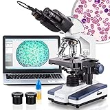
AmScope B120C-E1 LED Binocular Compound Microscope, 40X-2500X | $351.99 | Buy on Amazon |
- Trap the wire: Infrared laser beams acted as optical tweezers, holding the nanowire in place.
- Generate localized light: The wire’s nonlinear optical properties converted incoming laser light to a different frequency. Converted light emerged from the wire’s end, producing a small illumination source.
- Scan the sample: The researchers moved that source across the sample so it illuminated nanoscale structures locally.
- Record the image: A charge-coupled device (CCD) captured the resulting image.
The researchers described the approach as using an infrared laser to “optically trap and scan a nanowire over a sample.” The contemporary account is in Chemistry World’s 29 June 2007 report, which cites the original paper by Y. Nakayama and colleagues in Nature 447, 1098 (2007), DOI 10.1038/nature05921.
Free tools Windows power users keep installed
One-click scans. No signup required.
What does “subwavelength microscopy” mean here?
In this experiment, the term describes using a highly localized source of light to examine structures smaller than the scale that conventional far-field optical imaging can ordinarily resolve. Rather than relying only on light illuminating a broad area, the researchers scanned the nanowire’s emitting end across the sample. The wire therefore served as a tiny, movable “torch.”
#1 Best Overall
- Economical Microscope: The AmScope B120 Series is a high-quality, LED binocular compound microscope, an economical choice for both students and professionals
- Educational Value: Offering magnification from 40X to 2500X, this compound microscope excels in educational environments, labs, and clinics
- Illumination Excellence: Features LED light with a specialized fly-eye lens, providing bright, daylight-balanced illumination
- Digital Integration: Includes a 1.0 MP USB microscope camera with professional microscopy software for Windows, allowing for the capture and analysis of images
- About AmScope: We have the industry's leading collection of microscopes, microscopes cameras, accessories and other related products
Chemistry World reported that the setup distinguished structures with dimensions of a few tens of nanometres. It did not give a single standardized resolution figure in the accessible account, so that qualitative description should not be converted into a more precise resolution claim.
Independent reader supportYour contribution helps us test, update, and keep practical guides available for everyone.What the demonstration did—and did not—establish
The work brought together nanowire growth and characterization, optical trapping, parametric frequency conversion, scanning near-field microscopy and subwavelength measurement. Rob Eason of the University of Southampton’s Optoelectronics Research Centre called the combination a “tour-de-force,” while questioning whether it was ready for routine application.
The report discussed biology and other sciences as possible application areas, and the researchers suggested potential uses in physics, chemistry, materials science and biology. It also raised information storage or processing as a possible future direction. These were prospects, not evidence of routine deployment or a commercially available microscope. The account does not establish that the technique became a turnkey product.
How this differs from a later nanowire imaging method
A separate 2017 study used a fluorescent nanowire ring and film waveguide for wide-field far-field subdiffraction imaging. Its abstract reports resolving 70-nanometre-wide slots spaced 70 nanometres apart at 520 nanometres, with a viewing area up to 1000 μm2 (PubMed abstract). Those measurements belong to that later approach, not the 2007 scanned potassium niobate nanowire technique.
Quick Recap
Product prices and availability are accurate as of the date/time indicated and are subject to change. Any price and availability information displayed on Amazon at the time of purchase will apply.

