
iTechGuides is reader-supported. When you buy through links on our site, we may earn an affiliate commission. As an Amazon Associate I earn from qualifying purchases. Learn more
The iCEBreaker is an educational FPGA development board built around Lattice’s iCE40 UltraPlus 5K. It is intended for learning digital logic and building small FPGA projects—not as a drop-in replacement for a microcontroller. Its open-source learning focus, onboard programming interface, and PMOD expansion make it a practical starting point if you want to explore how hardware designs are synthesized and programmed.
What is the iCEBreaker FPGA?
The iCEBreaker is a development platform designed to teach and support open-source FPGA workflows. The project describes its aim as a “low cost, open-source educational FPGA development platform.” Its main chip is a Lattice iCE40 UltraPlus 5K in a QFN48/SG48 package. Unlike a microcontroller, an FPGA implements configurable digital logic: you describe a circuit, then build and load a bitstream that configures the chip.
The project’s official documentation positions the board for classes, workshops, and experimentation. The board’s resources are substantial for learning and small designs, but whether a particular design fits depends on its logic, memory, and timing requirements.
Recommended Free Tools
What hardware is on the board?
The official hardware documentation lists these FPGA resources and board interfaces:
#1 Best Overall

- Package Introduction: 1pc*【FPGA and PMOD-LED】
- ICE40UP5k main chip, 5280 LUT/128KB SPRAM/PLL/ SPI/I2C/DSP/PWM
- On-board iCELink debugger, supporting drag-and-drop programming, USB CDC serial port and JTAG
- Lead out all the IO with standard PMOD connector and can connect with other PMOD devices
- Totally use open source tool chain to develop
| Resource | Documented specification | What it means for a project |
|---|---|---|
| Logic | 5,280 logic cells | Configurable logic for implementing digital circuits; the available capacity does not by itself establish how large or fast a particular design will be. |
| Block RAM | 128 Kbit of dual-port block RAM | On-chip memory suited to designs that benefit from simultaneous access through two ports. |
| Single-port RAM | 1 Mbit (128 KB) | Additional on-chip memory resource; account for the design’s access pattern and total capacity. |
| DSP | Eight 16×16 DSP blocks | Dedicated arithmetic resources that can help with signal-processing and multiply-oriented designs. |
| Clocking and peripherals | PLL, internal oscillators, PWM capability, two SPI hard IPs, and two I2C hard IPs | Useful building blocks for clock generation and common digital interfaces; the exact design still determines how these resources are used. |
| Configuration flash | 128 Mbit (16 MB) QSPI-DDR-capable flash | Stores configuration or other data, with some associated pins shared with configuration and flash functions. |
| Programming and serial interface | FT2232H interface over micro-USB | Provides a connection for programming and serial connectivity through the board’s USB port. |
How much I/O does the iCEBreaker expose?
The hardware documentation describes 39 I/O-capable pins, but that figure should not be read as 39 interchangeable, uncommitted GPIO pins. The board allocates or shares pins among configuration and QSPI flash functions, RGB LEDs, the clock, UART, button, PMOD connectors, and connections to a snap-off section. Check the pinout and the functions your design needs before assigning signals; a pin used by one board feature may not be freely available for another.
How do you get started?
The official Getting Started guide points new users to the self-directed iCEBreaker Workshop and WTFpga materials. A typical open-source flow turns a hardware description into a programmed FPGA design through synthesis, place-and-route, and bitstream generation.
Rank #2

- Package Introduction: 1pc*【FPGA and PMOD-SDCARD】
- ICE40UP5k main chip, 5280 LUT/128KB SPRAM/PLL/ SPI/I2C/DSP/PWM
- On-board iCELink debugger, supporting drag-and-drop programming, USB CDC serial port and JTAG
- Lead out all the IO with standard PMOD connector and can connect with other PMOD devices
- Totally use open source tool chain to develop
- Choose a workshop or small design. Start with the official workshop materials so the exercise, required board connections, and expected result are clear.
- Check the tool instructions for your computer. The project has named Yosys, nextpnr, IceStorm, Icarus Verilog, and SymbiFlow among tools associated with its teaching goals. These are not necessarily all required for every workflow. Follow current tool documentation rather than assuming a historical setup guide still applies.
- Build the design. In the familiar flow described by the community wiki, Yosys performs synthesis, nextpnr handles place-and-route, and IceStorm tools generate the bitstream. Exact commands and setup depend on the chosen exercise and tool versions.
- Connect and program the board. Use the micro-USB connection and the project’s instructions for the selected programming workflow. The board’s FT2232H interface provides programming and serial connectivity.
- Verify the result, then add complexity. Confirm the first design behaves as expected before adding peripherals or expanding the logic. If the design fails to build or fit, inspect resource use, pin assignments, and timing constraints.
The community wiki’s operating-system advice is old: it recommended Linux or macOS and said Windows required more tool setup or Icestudio. Treat that as historical guidance, not a current compatibility guarantee; check the current tool documentation for installation steps and supported platforms.
What can you build with the iCEBreaker?
The board’s logic, RAM, DSP blocks, clocking, and common serial interfaces support learning digital design and developing small FPGA projects. The right fit depends on what the design needs: estimate its logic and memory use, identify required interfaces, and consider timing and pin availability. The listed specifications alone do not guarantee a particular clock rate or performance.
Rank #3

- Package Introduction: 1pc*【FPGA and PMOD Pack-1】
- ICE40UP5k main chip, 5280 LUT/128KB SPRAM/PLL/ SPI/I2C/DSP/PWM
- On-board iCELink debugger, supporting drag-and-drop programming, USB CDC serial port and JTAG
- Lead out all the IO with standard PMOD connector and can connect with other PMOD devices
- Totally use open source tool chain to develop
PMOD connectors let you add modules for a specific exercise or prototype. The PMOD documentation describes PMOD as a Digilent standard for connecting peripherals to FPGA development boards and lists categories including displays, DIP switches, DVI, gamepad/audio, HyperRAM, and LED panels. Older workshop examples use a 7-segment-display PMOD and a DIP-switch PMOD for WTFpga, and two 7-segment-display PMODs for the Stopwatch workshop. Those examples are tied to particular exercises; verify their current requirements before choosing hardware.
How should you choose a PMOD module?
Choose the module to match the project, not simply because it appears on a compatibility list. Before buying or wiring one, check:
Rank #4
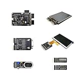
- Package Introduction: 1pc*【FPGA and PMOD Pack-3】
- ICE40UP5k main chip, 5280 LUT/128KB SPRAM/PLL/ SPI/I2C/DSP/PWM
- On-board iCELink debugger, supporting drag-and-drop programming, USB CDC serial port and JTAG
- Lead out all the IO with standard PMOD connector and can connect with other PMOD devices
- Totally use open source tool chain to develop
- Exercise requirements: Does the workshop or design call for that module, or can the same goal be met with onboard features?
- Connector population and pinout: Confirm the relevant connector is present and that the module’s signals map to pins your design can use.
- Electrical and interface needs: Check voltage and signal-interface requirements against the board and module documentation.
- Shared functions: Make sure the pins needed by the PMOD are not already committed to another board feature or design signal.
Who is the iCEBreaker for?
It is a sensible candidate for a learner who wants to understand digital hardware and follow a workshop-based, open-source FPGA flow. It can also suit small prototypes that fit the iCE40 UltraPlus 5K’s resources and available connections. It is less suitable if you are expecting a general-purpose microcontroller experience or need a guaranteed resource fit, performance level, or accessory setup without checking the project requirements.
Free tools Windows power users keep installed
One-click scans. No signup required.
Current stock, pricing, included accessories, and board-revision differences are not established by the project pages cited here. The hardware documentation identifies 1BitSquared as a place to obtain the board, but that does not confirm live inventory or what a current listing includes. No specific alternative board is evaluated here, so this is not a claim that the iCEBreaker is better than other FPGA development boards.
Quick Recap
Best Value

- Lead out all the IO with standard PMOD connector and can connect with other PMOD devices
- Features
- iCE40UP5k main chip, 5280 LUT/128KB SPRAM/PLL/ SPI///PWM
- On-board iCELink debugger, supporting drag-and-drop programming, USB CDC serial port and JTAG
- Totally use open source tool chain to develop
Product prices and availability are accurate as of the date/time indicated and are subject to change. Any price and availability information displayed on Amazon at the time of purchase will apply.

