
Recommended Free Tools
iTechGuides is reader-supported. When you buy through links on our site, we may earn an affiliate commission. As an Amazon Associate I earn from qualifying purchases. Learn more
A bias-reconfigurable barrier photodetector is a light sensor whose response changes when the voltage across its junction or interface is changed. In laboratory reports from 2023 to 2026, that single electrical control has been used to tune the wavelengths a device responds to, to switch a device between fast sensing and a slower, memory-like state, or to set an operating mode for ultraviolet detection.
The “barrier” in the name is the energy barrier at a junction or interface. Applied bias raises, lowers or reshapes that barrier, which governs how light-generated carriers are collected. The term is not a standardized detector class or a retail category. It describes a design approach that several laboratory groups are pursuing with different materials, so each device has to be judged on its own structure.
What bias changes inside the device
Applying a voltage does not do one thing. Depending on the material stack and junction design, the reported devices rely on one or more of four mechanisms:
Outdated Drivers Are Slowing You Down
One free scan finds every outdated or missing driver and matches the right update for your exact hardware.Free scan · exact hardware matchWindows Errors? Fix Them Before They Spread
Repair common Windows errors and clear accumulated junk for a smoother, more stable PC - no reinstall needed.Free scan · no reinstall- Carrier extraction. The electric field across the junction sweeps photogenerated electrons and holes toward the electrodes. Changing bias changes how quickly and how completely they are collected, which sets response speed.
- Carrier injection. Bias can push charge into the active layer from a contact, changing how many carriers are available to respond to light.
- Charge trapping. Carriers can be held in defect or interface states and released later. A carrier that stays trapped keeps influencing the output after the light has gone, which is one route to slow, memory-like behavior.
- Interfacial band alignment. Bias shifts the energy levels of the layers on either side of a junction, changing which photon energies are absorbed and collected. This is the mechanism behind the wavelength tuning in the hyperspectral imager discussed below.
The practical consequence is that a bias setting is not a universal sensitivity knob. Two devices driven at similar voltages can behave differently if their layers, interfaces or defect states differ, so the operating mechanism has to be read from each report rather than assumed from the title.
#1 Best Overall
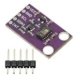
- High Accuracy I2C Particle Optical Sensor: Photodetectors board module designed for precise optical signal acquisition and particle detection applications
- Operating Voltage Specification: DC 5V power supply required for stable operation and reliable performance
- Communication Interface: IIC (I2C) protocol for easy integration with microcontrollers and development boards
- Compact Module Dimensions: 24.6 x 14.5mm board size with two M3 mounting holes for secure installation in various projects
- Wide Operating Temperature Range: Functions reliably in extreme conditions from -40C to +85C
The four reported devices at a glance
The table places the four reports side by side. Figures are given as each source reports them, with the conditions attached.
| Report (year, source basis) | Structure | Reported behavior | Reported figures and conditions |
|---|---|---|---|
| GaN optoelectronic micro-synapse (2026; PubMed article record, abstract) | Wafer-scale blue GaN micro-LED with a quantum-dot color-conversion layer | Red emission, self-powered detection at zero bias, bias-modulated synaptic plasticity | Response time of 91 ms at zero bias; carrier residence time extended 450-fold under applied bias (values reported by the authors for this device) |
| Hyperspectral quantum-dot image sensor (2026; Nature Photonics, version of record) | Monolithically integrated, stacked colloidal quantum-dot junctions | Hyperspectral imaging using bias-programmable band alignment and a bias-programmable spectral reconstruction algorithm | 400–1,700 nm coverage; 1 nm spectral resolution; 0.055 nm reconstruction accuracy; 1,280 × 1,024 spatial resolution; peak detectivity above 1013 Jones; 15 × 15 µm2 pixel footprint (reported by the authors) |
| AlScN/GaN UV heterojunction (2025; indexed abstract record, not the publisher page) | AlScN/GaN heterojunction | Bias-controlled modes for UV detection, imaging, optical communication and neuromorphic computing | Specific detectivity of 9.37 × 10¹² Jones at low bias (reported in the abstract) |
| Infrared nanocrystal film in a coupled Fabry–Pérot resonator (2023; ACS Photonics abstract) | Nanocrystal film in a coupled resonator, compared against standard interdigitated electrodes | Bias-switched spectral response | Effective absorption enhanced 30-fold versus standard interdigitated electrodes; spectral response switched by more than 25-fold by tuning bias below 1 V (reported in the abstract) |
Micro-synapse: fast detection and memory in one device
The GaN micro-synapse combines three functions in one structure. A blue GaN micro-LED is covered by a quantum-dot color-conversion layer that turns its emission red. The same structure detects light without an external bias, which the authors describe as self-powered operation. Bias then modulates its response in a way that resembles a synapse, the connection in neural circuits whose strength changes with activity.
Rank #2
- High Accuracy I2C MAX30105 Particle Optical Sensor Photodetectors Board Module Smoke Detection Flame Module 1.8V Power Supply
Bias is the link between the detection and memory functions. At zero bias the device responds quickly; under applied bias, carriers remain in the device far longer, which produces the slower, memory-like state. The two reported figures in the table are the clearest illustration in these reports of a speed-versus-retention trade-off: the state that responds fastest is not the state that holds the signal longest, and bias selects between them.
Quick wins for a faster PC:
Fix the driver behind crashes, sound loss and screen glitchesFind Drivers →Repair Windows errors before they cause bigger problemsFix Now →The platform is presented as relevant to neuromorphic vision, meaning sensors that process information in a way loosely modeled on neural tissue.
Rank #3
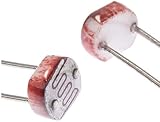
- A photoresistor or photocell is a light-controlled variable resistor.The resistance of a photoresistor decreases with increasing incident light intensity
- A photoresistor is also called light-dependent resistor (LDR), which can be applied in light-sensitive detector circuits, and light- and dark-activated switching circuits
- This is a very small light sensor and makes great ambient light triggers (when light in the room turns on, do something)
- Photoresistor is a resistor which made of semi-conductor material, and the conductance changes with luminance variation
- Yeah, this LDR can extend your projects at you limits. Imagine a system where the light of your house simply switch on / off depending on the sun light!
Hyperspectral imaging with bias-programmable band alignment
The quantum-dot imager reaches the same kind of control through a different structure. Its sensing layers are stacked colloidal quantum-dot junctions, and bias programs the band alignment between them. A spectral reconstruction algorithm, itself programmed by bias, then turns the device’s responses into a spectrally resolved image. Because the sensor is monolithically integrated, its stack is fabricated as one integrated unit rather than assembled from separate parts.
Two of the reported terms need context. Specific detectivity is measured in Jones, a unit normalized for device area and measurement bandwidth, so a higher value means a weaker optical signal can be distinguished from noise. The detectivity figure is a peak value, which describes the best operating point rather than performance across the full spectral range. The spatial and spectral figures are reported together, but the summary does not show whether each holds across the whole 400–1,700 nm span; the paper is the place to check that.
Rank #4

- Photo resistors, also known as light dependent resistors (LDR), are light sensitive devices most often used to indicate the presence or absence of light, or to measure the light intensity.
- In the dark, their resistance is very high, sometimes up to 1MΩ, but when the LDR sensor is exposed to light, the resistance drops dramatically, even down to a few ohms, depending on the light intensity.
- LDR has a sensitivity that varies with the wavelength of the light applied and is nonlinear device.
- They are used in many applications but are sometimes made obsolete by other devices such as photodiodes.
- Please check the right type to meet your needs.
The authors suggest food-quality monitoring, chemical-solvent discrimination and material identification as possible uses. These are proposed applications, and no field validation of any of them is reported.
UV and infrared reports: bias as an operating-mode switch
AlScN/GaN UV heterojunction (2025)
The indexed abstract describes bias-controlled operating modes spanning UV detection, imaging, optical communication and neuromorphic computing. The significance for a reader is that one heterojunction is presented as serving several roles depending on bias. Whether each role is demonstrated to the same depth is a question the full article answers, and the abstract alone does not.
Best Value

- Adopting a slot type photoelectric sensor, it consists of an infrared light-emitting diode and an NPN photoelectric transistor, with a slot width of 5.9mm.
- As long as a non-transparent object passes through the slot, it can trigger to output a low TTL level.
- Using Schmidt trigger to jitter pulses is very stable and can be used for small car speed measurement, distance measurement, and other applications!
- Install holes with M3 screws at both ends.
- Working voltage: 3.3V-5V, output form: digital switch output (0 and 1)
The detectivity value is quoted at low bias, and that condition is part of the number. A detectivity taken at a different bias should not be set beside it as if both were measured under the same conditions.
Infrared nanocrystal film in a Fabry–Pérot resonator (2023)
In this design, bias tunes the spectral response in the infrared. The nanocrystal film sits in a coupled Fabry–Pérot resonator, an optical cavity that confines light so it makes repeated passes through the absorbing film. The enhancement is measured against a standard interdigitated electrode layout without the resonator, so the result describes this specific combination of film, resonator and electrodes rather than nanocrystal detectors in general.
The tuning range is reported as bias below 1 V. The abstract does not report power consumption, so any statement about energy use for this device is not established.
How to compare these devices
Compare the devices on the axes below rather than ranking them on headline figures. The four reports were not tested against one another, and each figure depends on its own wavelength range, geometry, bias and measurement conditions.
Quick Recap
- Wavelength coverage: ultraviolet, infrared, or the 400–1,700 nm broadband range.
- Spatial and spectral resolution, where the device forms an image.
- Response time and retention, which together set the balance between fast sensing and memory.
- Bias voltage and the bias range over which the device changes behavior.
- Detectivity, always read together with its bias condition.
- Pixel footprint and integration level, including whether the sensor is monolithically integrated.
- Fabrication route and the task actually demonstrated, such as imaging, synaptic behavior or communication.
What is and is not established
- Commercial availability. None of the four reports establishes a purchasable detector, accessory, replacement part or fabrication kit for this application. The devices described are laboratory structures.
- Deployment. The food-quality, solvent-discrimination and material-identification uses are proposals. The UV and neuromorphic modes are demonstrations of device behavior, not deployed systems.
- Market size and adoption. The reviewed evidence contains no market, adoption or deployment statistics. The numbers in this article describe device performance and should not be read as measures of demand.
- Generalization. Each figure belongs to one device, one geometry and one measurement condition. The response time, retention gain and absorption enhancement reported above do not describe bias-reconfigurable detectors as a class.
- Method depth. The GaN and UV figures come from abstract-level records, and the infrared figures come from a publisher abstract. Test conditions, error analysis and full methods sit in the complete articles, which should be checked before any number is quoted.
”
The Bottom Line
“”
Product prices and availability are accurate as of the date/time indicated and are subject to change. Any price and availability information displayed on Amazon at the time of purchase will apply.

