
iTechGuides is reader-supported. When you buy through links on our site, we may earn an affiliate commission. As an Amazon Associate I earn from qualifying purchases. Learn more
Advanced packaging can limit AI-accelerator output even when compute dies have been fabricated: a finished module also needs high-bandwidth memory (HBM), interposers, substrates, specialized materials, and qualified packaging capacity to come together. The constraint is a linked supply system, not one factory step. Manufacturers are responding with planned facility expansions, additional suppliers for selected inputs, and larger-package technologies—but announcements and forecasts are not the same as operating, qualified production.
Why packaging capacity can limit accelerator output
In 2.5D integration, multiple dies are assembled side by side and connected through a high-density interposer, with HBM stacks incorporated into the same package. TSMC describes its CoWoS technology as a 2.5D packaging approach for high-performance computing (HPC) and AI. Its 2025 annual report says the technology integrates multiple system-on-chip dies with HBM to increase compute capability and memory bandwidth.


This makes packaging a production constraint in its own right. A fabricated compute die is not a finished accelerator if the memory, interposer, substrate, materials, assembly equipment, and qualified packaging line needed for integration are not available together. Advanced packaging capacity is therefore distinct from wafer-fab capacity: more fabricated chips alone do not necessarily mean more completed accelerator modules.
What’s actually slowing this PC down?
Pick the symptom - the matching free tool is one click away.
Where the bottlenecks arise
Specialized integration and concentrated demand
AI accelerators put pressure on packaging processes that must connect multiple compute dies and HBM stacks using dense interconnects. That work is more specialized than generic assembly. TrendForce’s April 2026 analysis attributes sustained CoWoS tightness to the rapid increase in AI demand since 2023. It also characterizes the supplier concentration as temporary; that is the analyst’s assessment, not a measured market-share figure.
#1 Best Overall
TrendForce says customers began securing wafer capacity, CoWoS, HBM, substrates, and other materials ahead of need. The report characterizes many chip designs as being finalized one to three years in advance. That is an industry assessment, not a universal design-cycle rule, and the report does not establish that every early commitment is a binding purchase order. Early reservations can still make available capacity harder to obtain for customers who come later.
A missing input can idle the rest of the chain
TrendForce identifies production equipment, substrates, packaging materials, and other critical components as constraints beyond CoWoS service capacity. The dependencies can be understood as a chain:
Rank #2

- Designed for 6 inch wafer processing applications, providing stable support for semiconductor wafers during handling and manufacturing.
- Suitable for semiconductor Fab environments, wafer inspection, chip packaging and related production processes.
- Precision manufactured wafer ring frame with consistent dimensions, helping improve wafer handling efficiency and operational stability.
- 6-inch standard wafer ring T=1.2mm Material: SUS420 Selection
- Used as a supporting frame for wafer transfer, processing and storage to reduce handling difficulty during semiconductor workflows.
- Package design and qualification establish which components and interconnects must work together.
- Compute dies and HBM must be available in the required configurations.
- Interposers, substrates, and packaging materials must match the design and be supplied in time.
- Packaging and assembly equipment must be available to integrate the components.
- The assembled package must complete integration and qualification before it can count as finished output.
This is an explanatory map of the dependencies, not a published production flow chart. The available evidence does not provide comparable current figures for substrate capacity, HBM output, equipment lead times, yields, labor, or electricity across suppliers, so it does not support ranking these constraints by relative importance. ASE and WUS’s planned Kaohsiung project includes a high-voltage substation, but that detail alone does not demonstrate a sector-wide power shortage.
Capacity takes time to build and qualify
Announcing a site or line does not immediately add qualified production. A facility must be built, equipped, qualified for the relevant processes and customer products, and ramped. The announcements discussed below describe plans, agreements, or technology development; they do not establish present utilization or a universal time to reach high-volume output.
Rank #3
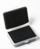
- PE foam storage box designed for IC chips, semiconductor components, optical parts, crystals, glass parts and PCB samples.
- Compact structure with internal foam layers helps reduce shaking and vibration during storage and transportation.
- Made of PE material with clean surface, corrosion resistance, moisture resistance and reliable protection performance.
- Set includes 1 plastic box and 2 foam inserts, featuring snap closure design with black base and transparent cover.
- Suitable for semiconductor laboratories, electronics manufacturing, component storage, sample display and precision device transportation.
Capacity decisions also involve lead times. TrendForce’s one-to-three-year characterization of design finalization helps explain why customers and suppliers may plan ahead, but the report does not quantify the risk that expected demand will differ from realized demand.
How manufacturers are responding
| Response | Constraint it targets | Status and what is established |
|---|---|---|
| Amkor Arizona campus expansion | Packaging and test cleanroom space in the United States | Amkor’s September 2026 announcement describes planned phase-one cleanroom space of 33,000 square meters and says phase two is expected to add 60,000 square meters, for about 93,000 square meters across the campus. The company said phase-two customer commitments exceeded the phase-one area. These are company plans and commitments, not verified operating capacity or output. |
| TSMC advanced packaging facilities and CoWoS development | Packaging capacity and package architecture for larger products | TSMC’s 2025 annual report describes CoWoS, InFO, SoIC, and COUPE, and says the company intends to add advanced packaging facilities as part of its U.S. manufacturing investment. It also describes CoWoS-L, which combines an RDL interposer with embedded local silicon interconnect. The report said products using larger-reticle interposers were expected to begin volume production in 2026; that is an expectation stated in the report, not confirmation here that the ramp occurred. |
| ASE and WUS Kaohsiung hub | Regional packaging ecosystem capacity and options for AI products | The companies announced a planned hub for advanced AI packaging. Their announcement names chip stacking, chiplet integration, CoWoS, and FOCoS, and frames demand around HPC, cloud services, and data centers. It does not establish the project’s eventual throughput or customer qualification status. |
| GlobalFoundries silicon-interposer supply agreement with TSMC | Availability and geographic diversity of one CoWoS input | The companies announced a five-year initial agreement to establish U.S.-based silicon-interposer supply for TSMC’s CoWoS ecosystem, with a framework for future expansion. This adds a planned source for interposers; it does not relocate or replace all CoWoS operations, materials, or suppliers. |
| ASE panel-level packaging development | Potential scale and efficiency for heterogeneous integration | ASE announced development of an automated 310 mm × 310 mm panel-level packaging production line in May 2026. The announcement presents panel processing as a scalability and efficiency approach, but does not establish volume output, yield, cost per package, or equivalence to wafer-level interconnect density. |
Facility expansion: more space, with a qualification gap
Amkor’s Arizona plan addresses packaging and test space, while TSMC’s stated U.S. investment intent addresses advanced packaging facilities within its broader manufacturing plans. Such expansions can add options and geographic capacity if they are completed and qualified. The announced square-meter figures describe planned cleanroom area, not the number of accelerator packages a site can produce.
Rank #4
Supply diversification: targeted relief, not a complete alternate chain
The GlobalFoundries agreement targets silicon interposers specifically. It is a diversification step for one input in TSMC’s CoWoS ecosystem, rather than a substitute for HBM, substrates, other materials, assembly lines, or the full package process. The ASE-WUS hub is a broader collaboration announcement, but its eventual capacity and qualification remain unstated in the announcement described here.
New package formats: a possible scale path, not a drop-in replacement
ASE’s panel-level work and TSMC’s CoWoS-L development are different approaches to scaling. The panel project is in development; the available announcement does not show that it is already delivering high-volume production or matching wafer-based density. CoWoS-L instead extends TSMC’s wafer-based approach with an RDL interposer and embedded local silicon interconnect. TSMC’s 2025 report attached a 2026 expected volume-production start to products with larger-reticle interposers, rather than reporting a verified production result.
Best Value

- Selfadhesive safety: the silicone chip storage case features an innovative selfadhesive internal structure, securing semiconductor and silicon die chips against shifting or abrasion during lab movements,laboratory chip container,lab chip container
- and safe handling: engineered as a laboratory sample carrier with a smooth, easy surface, it edge abrasion and , making it suitable for semiconductor sample and die protection,die transport box,chip preservation box
- Efficient space management: the chip collection storage box supports orderly batch stacking, optimizing space utilization and enabling systematic research sample organization for busy labs,semiconductor chip storage box,chip storage and transport box
- Contact damage minimization: the protective chip transport case presents a polished, burrfree surface, reducing edge wear and supporting safe handling of micro components and wafer samples,chip packaging box,micro component storage box
- Flexible lab compatibility: as a micro sample storage box, its compact build matches most laboratory storage and transport carts, facilitating effortless movement across different workstations and environments,research sample storage box,sample chip carrier
What the forecasts do—and do not—say
TrendForce reported in June 2026 that TSMC CoWoS capacity was forecast to grow at more than 80% compound annual growth from 2022 to 2027, attributing the forecast to TSMC’s May 2026 technology symposium. This is a forward-looking growth forecast, not a realized capacity increase or a measure of total global advanced-packaging capacity.
In the same June 2026 outlook, TrendForce expected expansion to narrow the supply-demand gap and said severe 2.5D packaging shortages might moderate from 2027. That is a dated analyst forecast, not evidence that the bottleneck has been solved. Demand, project execution, qualification, and the availability of linked inputs all affect whether planned capacity becomes finished-package output.
The announcements and forecasts provide no comparable, independently measured figure for current global advanced-packaging capacity or utilization. As a result, the specific responses can be compared by what they target and how mature they are, but not combined into a reliable global capacity total.
Quick Recap
Product prices and availability are accurate as of the date/time indicated and are subject to change. Any price and availability information displayed on Amazon at the time of purchase will apply.

