
iTechGuides is reader-supported. When you buy through links on our site, we may earn an affiliate commission. As an Amazon Associate I earn from qualifying purchases. Learn more
A silicon wafer is only the starting substrate. The difficult work is building reliable, microscopic layers on it, aligning every layer, finding defects, correcting the process and finally packaging dies that work consistently. ASML says chip manufacturing involves hundreds of steps and can take up to four months from design to mass production.
That is why “silicon is the easy part” is a useful shorthand. The material is abundant and well understood; manufacturing a high-yield integrated circuit is a tightly controlled chain of lithography, deposition, etching, modification, measurement, inspection, software correction and packaging.
What a silicon wafer actually provides
A polished wafer provides a uniform surface on which transistor structures and interconnects can be formed. It does not contain a functioning processor, memory device or accelerator by itself. The circuit emerges only after many patterned layers are built and connected.
PC Slower Than It Used to Be?
A free scan shows the junk files, broken settings and background clutter dragging Windows down - then fixes them in one click.Free scan · Windows 10 & 11Outdated Drivers Are Slowing You Down
One free scan finds every outdated or missing driver and matches the right update for your exact hardware.Free scan · exact hardware matchEach layer must land in the right place, use the right materials and remain clean enough that microscopic contamination does not create a failure. A finished wafer therefore represents a history of process conditions, measurements and corrections, not just a piece of silicon.
#1 Best Overall

- TURN CODE INTO REAL-WORLD RESULTS — Follow 22+ guided lessons to make LEDs blink, read temperature and distance, move servo and stepper motors, control an LCD and respond to joystick or IR input; ideal for a family weekend build, homeschool unit, coding club or STEM classroom
- MORE PROJECT VARIETY IN ONE ORGANIZED KIT — Includes the UNO R3 controller, LCD1602 with pre-soldered header, breadboard power module, ultrasonic and DHT11 sensors, joystick, IR receiver and remote, SG90 servo, stepper motor, relay, DC motor, fan blade, displays, LEDs, buttons, resistors and jumper wires
- START WITHOUT SOLDERING — Plug-in modules, a solderless breadboard and the pre-soldered LCD help beginners focus on wiring, code and testing; the illustrated component list makes it easier to find each part and move from one lesson to the next
- LEARN THE LOGIC, THEN CREATE YOUR OWN — Use Arduino IDE and the included example code to understand digital input and output, analog sensing, timing, motor control and display functions, then change thresholds, speeds and sequences for alarms, environmental monitors, reaction games and motion projects
- CLEAR SETUP SUPPORT FOR FIRST-TIME BUILDERS — Download the latest tutorial and code, select the UNO board and correct computer port, check component polarity and breadboard rows, and keep power-module input at 9V or below; younger learners should work with an experienced adult
What happens after the wafer is made?
- Coating: The wafer is covered with a light-sensitive material, commonly called photoresist, so a pattern can be transferred.
- Exposure: A lithography system projects a mask pattern onto the resist. The optical image is deliberately corrected because the printed result is affected by optical, physical and chemical effects.
- Development: The exposed resist is developed so selected regions remain or are removed, creating a temporary pattern.
- Etching and material changes: Exposed areas are etched, doped or otherwise modified. Other steps deposit films that become part of the device.
- Measurement and inspection: Metrology checks dimensions, overlay and other process results; inspection looks for defects. The data feeds corrections rather than serving only as a final pass/fail check.
- Layer repetition: The coat, expose, develop, modify, measure and inspect cycle is repeated for the many layers that form transistors and interconnects.
- Dicing and packaging: The completed wafer is separated into individual dies. Working dies are packaged and tested so they can connect to a circuit board or larger system.
The exact recipe varies by device and manufacturing technology, but the central challenge remains the same: every new layer must meet its own specifications without compromising the layers underneath.
Why lithography is a precision-and-correction problem
Lithography is often described as printing, but ordinary printing is a poor analogy for advanced chips. The desired pattern is altered by the limits of optics, the behavior of materials and the chemistry of development. The machine and the mask therefore cannot simply reproduce the design file literally.
Computational lithography uses manufacturing models calibrated with test-wafer data to predict those distortions and change the pattern before exposure. The correction is part of the manufacturing flow: the mask is designed so that the wafer, after the physical and chemical effects occur, ends up closer to the intended geometry. ASML states that without computational lithography it would be impossible for chipmakers to manufacture the latest technology nodes.
Quick wins for a faster PC:
Scan for outdated or missing drivers - takes under a minuteDriver Scan →Repair Windows errors before they cause bigger problemsFix Now →Fix the driver behind crashes, sound loss and screen glitchesFind Drivers →Rank #2

- 35+ Guided Electronics Projects: Progress from LEDs and buttons to RFID access, real-time clocks, motion and distance sensing, environmental monitoring, motor control and interactive displays for STEM learning, coding clubs and maker projects
- More I/O and Memory for Larger Builds: The MEGA 2560 R3 provides 54 digital I/O pins, including 15 PWM outputs, 16 analog inputs, 4 hardware serial ports and 256 KB flash for projects that combine more sensors, controls and displays
- 200+ Components for Prototyping: Includes LCD1602, RC522 RFID, RTC, DHT11, HC-SR501 PIR, ultrasonic and water-level sensors, GY-521, MAX7219, keypad, joystick, rotary encoder, relay, SG90 servo, stepper motor, DC motor, breadboard and more
- Learn, Modify and Create: Follow 35+ guided lessons with example code, then adjust sensor thresholds, timing, display text, motor behavior and control logic to turn structured exercises into access systems, monitors, alarms and interactive projects
- Organized for Repeatable Learning: Pre-soldered modules, a solderless breadboard, storage case and small-parts box reduce setup time and keep sensors, LEDs, ICs, wires and other components easy to find between projects
Alignment and motion are engineering problems of their own
A chip contains multiple patterned layers, so overlay—the placement of one layer relative to another—must remain within an extremely small error budget. ASML describes sensors measuring positioning 20,000 times per second with 60-picometer accuracy. Those figures describe the control challenge, not a guarantee that every feature on every wafer has exactly that error.
The motion system must also keep production practical. In an ASML lithography machine, the stage moves two wafer tables simultaneously, with each table holding a silicon wafer. Parallel handling helps expose one wafer while another is being prepared, but it adds synchronization, vibration-control and thermal-management requirements.
Why yield matters more than a successful demonstration
A single working die proves that a design and process can function. A commercial fab must produce a high proportion of working dies across many wafers, lots and production days. A defect, dimensional drift or alignment error can reduce the number of sellable chips even when most of the wafer appears correct.
Rank #3
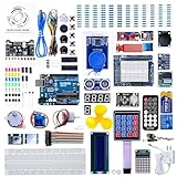
- 30+ Guided Electronics Projects: Start with LEDs and build toward LCD1602 displays, RFID access, motion detection, distance sensing, motor control and environmental monitoring for STEM learning, coding clubs, classrooms and hobby projects
- 200+ Components Across 63 Types: Includes an ELEGOO UNO R3 controller, LCD1602, RC522 RFID, RTC, HC-SR501 PIR sensor, ultrasonic sensor, DHT11, GY-521, MAX7219, keypad, joystick, relay, SG90 servo, stepper motor, breadboard and more
- Begin Without Soldering: Pre-soldered modules, a solderless breadboard, organized storage case and small-parts box reduce setup time and help beginners move from lesson to lesson while keeping LEDs, ICs, wires and sensors easy to find
- Learn, Modify and Create: Program the ELEGOO UNO R3 board with Arduino IDE using the included PDF tutorial and example code, then adjust sensor thresholds, timing, display text and motor behavior to turn guided lessons into original projects
- Flexible Power and Project Setup: Includes a 9 V, 1 A power supply, breadboard power module, 9 V battery and USB cable to support controller, breadboard and module experiments without sourcing basic setup accessories separately
Yield improvement is therefore a feedback system. TSMC describes intelligent detection, diagnosis, self-learning and process management spanning wafer fabrication through die packaging. In practical terms, data from inspection and tests is used to identify the likely cause, adjust the process and check whether the correction worked. No single lithography exposure, deposition tool or inspection image can provide that result alone.
Free tools Windows power users keep installed
One-click scans. No signup required.
Contamination control is part of the product
Particles and chemical contamination can damage structures that are too small to see with ordinary inspection. ASML says its cleanrooms are about 10,000 times cleaner than outside air and describes ISO class 1 conditions with no more than 10 particles between 100 and 200 nanometres per cubic metre. Such controls protect the repeatability of every process step; they are not cosmetic features of the facility.
The manufacturing ecosystem is larger than the fab floor
Advanced production depends on equipment makers, materials suppliers, software developers, metrology and inspection specialists, packaging providers and the chip manufacturer’s own process engineers. ASML’s 2025 annual-report material lists more than 44,000 employees and 5,100 suppliers, illustrating the scale of one major equipment company’s industrial network. Those numbers are not a count of the entire semiconductor industry, but they show why a leading process cannot be recreated by buying one machine.
Rank #4
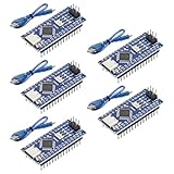
- Powerful: The Arduino Nano V3.0 Board Microcontroller Built with ATmega328P and CH340 chips instead of FT232, Improved new version CH340G Replace FT232RL, making it ideal for beginners
- Seamless Compatibility: Fully compatible with Arduino Nano, supporting Arduino IDE, ISP programming and USB download. Works seamlessly with Windows, Mac, and Linux operating systems for a hassle-free experience.
- Versatile I/O & Compact Design: Features 14 digital I/O pins (6 PWM outputs), 6 analog inputs, a 16MHz quartz oscillator, USB-C power socket, ICSP port, and reset button. Its compact, breadboard-friendly design ensures easy handling and integration.
- Flexible Power Supply Options: Supports multiple power sources, including USB-C, 6-12V unregulated external power, or 5V regulated external power. The Nano board intelligently switches to the higher voltage source automatically—no jumper selection required.
- Excellent Communication Capabilities: Designed for seamless communication with PCs and arduino microcontrollers, the Nano board is fully compatible with multiple operating systems and offers stable and reliable performance for a variety of projects.
Is the hard part chip design, the fab or the software?
There is no single answer because the three layers solve different failure modes:
| Layer of the system | Core problem | What success requires |
|---|---|---|
| Chip design | Specify a circuit that is functionally correct and manufacturable. | Accurate layouts, electrical rules and designs that tolerate real process variation. |
| Fabrication | Turn layouts into repeatable physical structures at useful yield. | Patterning, alignment, materials control, inspection, feedback and contamination control. |
| Software and system support | Make the finished silicon usable by applications and customers. | Drivers, runtimes, documentation, tools and support that expose the hardware’s capabilities. |
The phrase “silicon is the easy part” usually points at the gap between a physical chip and a dependable product. A design can be elegant yet difficult to manufacture; a wafer can contain working dies yet fail to deliver acceptable yield; and an accelerator can be powerful yet difficult to use without the surrounding software.
What to look for when judging a manufacturing approach
Claims about a process, tool or supplier should be examined across several dimensions rather than reduced to a single feature size:
Best Value
![Arduino Uno REV3 [A000066] - ATmega328P Microcontroller, 16MHz, 14 Digital I/O Pins, 6 Analog Inputs, 32KB Flash, USB Connectivity, Compatible with Arduino IDE for DIY Projects and Prototyping](https://m.media-amazon.com/images/I/515P6aYSP4L._SL160_.jpg)
- ATmega328P Microcontroller: Powered by the reliable ATmega328P, running at 16 MHz with 32KB of flash memory, 2KB SRAM, and 1KB EEPROM, offering ample resources for a wide range of basic to advanced electronics projects.
- 14 Digital I/O Pins & 6 Analog Inputs: Features 14 digital I/O pins (6 of which support PWM output) and 6 analog inputs (10-bit resolution), providing flexible options for sensors, motors, and other external components.
- USB Connectivity for Easy Programming: The built-in USB port allows for direct programming and serial communication, enabling a simple connection to your computer for sketch uploading and debugging through the Arduino IDE.
- Compatible with Arduino IDE: Full compatibility with the Arduino IDE ensures easy access to a vast array of libraries, code examples, and community-driven projects, making the Uno a great choice for both beginners and experienced makers.
- Widely Used in Education & Prototyping: The Arduino Uno is a standard in educational environments, widely used for learning and teaching electronics and programming. It's perfect for prototyping, robotics, IoT projects, and more.
- Patterning resolution and the width of the usable process window.
- Overlay and alignment accuracy across all critical layers.
- Throughput and cost per good die, not just peak machine capability.
- Metrology, defect detection and the speed of feedback into the process.
- Computational correction and the quality of the models behind it.
- Contamination control and the stability of materials and equipment.
- Packaging and integration capability after wafer fabrication.
- Supply-chain resilience for specialized tools, parts and materials.
These criteria explain why semiconductor progress is cumulative. Better hardware helps, but yield comes from coordinating optics, mechanics, chemistry, software, measurement, people and suppliers over hundreds of controlled steps.
The bottom line
Silicon is the substrate, not the finished technology. The hard part is repeatedly transforming that substrate into aligned, inspected and packaged structures while correcting errors quickly enough to achieve high yield. That combination of precision engineering, computational modeling, process feedback and industrial coordination is what turns a wafer into a reliable chip.
Quick Recap
Product prices and availability are accurate as of the date/time indicated and are subject to change. Any price and availability information displayed on Amazon at the time of purchase will apply.

