
PC Slower Than It Used to Be?
A free scan shows the junk files, broken settings and background clutter dragging Windows down - then fixes them in one click.Free scan · Windows 10 & 11Outdated Drivers Are Slowing You Down
One free scan finds every outdated or missing driver and matches the right update for your exact hardware.Free scan · exact hardware matchiTechGuides is reader-supported. When you buy through links on our site, we may earn an affiliate commission. As an Amazon Associate I earn from qualifying purchases. Learn more
“I²C noise” describes a symptom, not a diagnosis. A bus that produces NACKs, corrupted bytes, or intermittent lockups may have electrical interference, slow edges, ringing, incorrect pull-ups, a stuck device, or a protocol problem. Start by measuring SDA and SCL at the device pins with an oscilloscope; decoded bytes alone cannot show why a transaction failed.
What noise on an I²C bus looks like
I²C uses bidirectional SDA and SCL lines. In ordinary operation, devices pull a line low and release it; pull-up resistors create the high level. A waveform can therefore fail without looking like random spikes: an overloaded bus may simply rise too slowly, while a long cable or poor probe connection may produce ringing.
Spikes and threshold recrossings
A brief disturbance may come from crosstalk, switching-current coupling, ESD, a connector, or the measurement setup. It matters most if it crosses the receiving device’s input threshold or creates an extra transition. A logic analyzer may decode such a crossing as an extra clock or malformed byte. Compare the glitch with the device’s specified thresholds and any documented input filtering; filtering is not universal.
Free tools Windows power users keep installed
One-click scans. No signup required.
Ringing and overshoot
Ringing after an edge can point to reflections from cables, connectors, long branches, or stubs, or to an unsuitable probing connection. Overshoot and undershoot can also threaten device pin limits. Try a short probe ground spring or a suitable coaxial connection; if the waveform changes markedly, the probe setup is part of the problem.
#1 Best Overall
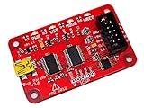
- USB interface, USB powered. 5volt tolerant pins. 0-6volt measurement probe. 1Hz-40MHz frequency measurement. 1kHz-4MHz pulse-width modulator, frequency generator. On-board multi-voltage pull-up resistors.
- On-board 3.3volt and 5volt power supplies with software reset. Macros for common operations. Bus traffic sniffers (SPI, I2C). Transparent USB to serial bridge mode. 10Hz-1MHz low-speed logic analyzer. Custom support in AVRDUDE , Flashrom , OpenOCD.
- AVR STK500 v2 programmer clone. Scriptable from Perl, Python, etc. A bootloader for easy USB firmware updates. Uses DP6037 standard PCB layout. Open source (CC 0/Public Domain).
Slow, rounded rising edges
A slow rise is often the expected resistor-capacitor response of a heavily loaded bus, not random noise. It can still reduce timing margin and leave a receiver in its threshold region longer, making the line more susceptible to interference. Measure rise time between the specification’s measurement thresholds—commonly 30% and 70% of the supply—not simply from zero to the rail. Microchip’s pull-up guidance describes this measurement and the related resistor calculations.
Unexpected SDA changes or a line held low
In normal signaling, SDA changes while SCL is high for START and STOP conditions. Other changes may indicate a glitch, contention, timing violation, or device behavior the decoder does not understand. A line that stays low while idle is a different clue: a device may still be sinking it, the line may be shorted, or a translator or power-sequencing problem may be blocking release.
Why the physical layer is vulnerable
Because devices normally do not drive the high level, the pull-up resistor must charge the total capacitance of pins, traces, connectors, protection components, translators, muxes, and any cable. A larger resistor lowers the current devices must sink but slows the rise. A smaller resistor speeds the rise but demands more sink current and can violate a device’s VOL or IOL limits. Long wiring and additional devices increase capacitance and can reduce the usable bus speed; Analog Devices’ I²C cabling guidance discusses that trade-off.
Not every apparent noise problem is interference. A clock-stretching device can legitimately hold SCL low; an incorrect pull-up voltage can exceed a peripheral’s limits; parallel module pull-ups can make the effective resistance too small; and a push-pull output configured to drive high can fight a device pulling low. Firmware resets, addressing errors, or a slave left mid-transaction can also cause failures that resemble noise.
Rank #2
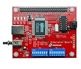
- 【46 Protocol Simulations】Generates CMD, CLK, and DATA signals for 46 common protocol packet formats.
- 【Perfect for Learning】Designed for beginners and students to study and understand digital communication protocols.
- 【Compatible with Logic Analyzers】Works with Zeroplus Logic Analyzers to quickly decode and visualize signal behavior.
- 【Educational and Practical】Ideal for microcontroller training, bus communication lessons, and lab use.
- 【Compact and Easy to Use】Portable design, simple setup, and ready for hands-on practice.
I²C timing limits to check
The following values are from NXP’s UM10204 specification table. Confirm the applicable specification revision and every participating device’s datasheet before treating them as design limits; a nominal clock rate or capacitance figure does not establish that a particular cable topology will work.
| Mode | Nominal maximum clock rate | Maximum rise time | UM10204 typical maximum bus capacitance |
|---|---|---|---|
| Standard-mode | 100 kHz | 1,000 ns | 400 pF |
| Fast-mode | 400 kHz | 300 ns | 400 pF |
| Fast-mode Plus | 1 MHz | 120 ns | 550 pF |
The same specification gives high- and low-level noise-margin figures of approximately 0.2 VDD and 0.1 VDD for the listed modes, and notes input filtering for spikes shorter than 50 ns in relevant devices. This is not a guarantee that every controller, sensor, translator, or mux filters every such disturbance. Check the actual parts and their voltage domains. See NXP UM10204.
How to troubleshoot an unreliable bus
- Record the failure. Note the failing address and operation, whether it occurs at an ACK, read, write, repeated START, or clock-stretch interval, and whether it correlates with temperature, cable movement, motors, displays, radios, or converter activity. Record whether the bus recovers after reset and whether either line remains low.
- Inspect the unpowered wiring and power domains. Check SDA, SCL, and ground continuity; connector pinout; pull-up locations; translator orientation; and whether any output is configured push-pull. Identify every module’s pull-ups and calculate their parallel equivalent. Confirm that pull-ups go to a voltage every connected device can tolerate, and check whether an unpowered device can obstruct or be back-powered through its I/O pins. NXP’s UM10204 discusses powered-off device behavior.
- Check idle levels. With no transaction active, SDA and SCL should normally be high. Measure the actual high voltage and look for ripple, periodic spikes, or low-frequency movement. Compare the controller end with the farthest device, and repeat with suspected switching loads enabled and disabled.
- Capture SDA and SCL analog waveforms during a failure. Use two oscilloscope channels, a short ground connection, adequate sample rate and bandwidth, and a trigger on the failing transaction or suspect edge. Protocol decoding helps correlate the waveform with the transaction but cannot explain analog ringing or threshold margin by itself. Tektronix describes oscilloscope triggering and I²C decoding in its I²C and SPI troubleshooting note.
- Measure rise time, fall time, and low level at the receiver. Compare SDA and SCL rise times with the selected mode and part limits. Check fall time, VOL under the strongest combined pull-up load, and overshoot or undershoot against pin ratings. Determine whether any disturbance crosses the receiving device’s thresholds.
- Probe multiple locations. Check at the controller, a nearby device, and the farthest device; for a translated or buffered bus, inspect both sides. A clean controller waveform and degraded remote waveform point toward wiring, branches, ground reference, or the segment interface.
- Change one variable at a time. Temporarily lower SCL frequency, shorten the cable, remove an optional device, disable a switching subsystem, or test a different probe. Record the result before changing another variable. This isolates the cause rather than masking it.
Choose pull-ups from the bus, not a rule of thumb
For a first-order estimate, the rise time is approximately:
Recommended Free Tools
tr ≈ 0.8473 RPCBUS
That gives a maximum pull-up resistance for a specified rise-time limit:
Rank #3

- CAN Mode: Automatic regonize the direction of CAN-H and CAN-L, can read CAN BUS Baud Range: 50, 83, 100,125,150,200,250,300,400,500,666,800,1000kbps
- LIN Mode: can read LIN BUS Baud Range: 2400-4800-9600-14400-19200bps. Red plug connects to LIN, black plug connects to GND.
- PWM Singal Mode: < 20V PWM singal detector for line.
- View Standard Frames ID data: Easy to stop the ID page to read the part of standard frames data.
- Directly use CAN/LIN/PWM analyzer quickly check if the plug with communication data or not.
RP(max) = tr / (0.8473 CBUS)
The minimum resistance is constrained by the current the device can sink while meeting its low-level voltage requirement:
RP(min) = (VDD − VOL(max)) / IOL
Use total bus capacitance, the required rise time, the pull-up supply, and the weakest participating device’s sink specification. Microchip’s external pull-up selection guidance gives these constraints.
Illustrative Fast-mode calculation
For an illustrative 200 pF bus and a 300 ns rise-time limit, the upper-bound calculation is 300 ns ÷ (0.8473 × 200 pF), or approximately 1.77 kΩ. This is not a universal resistor recommendation: the selected value must also satisfy the minimum-resistance constraint and the sink-current limits of every device that can pull the line low.
The Tool Desk
Outbyte PC Repair FREEClear out junk files and repair common Windows errorsFree Scan →Outbyte Driver Updater FREEScan for outdated or missing drivers - takes under a minuteDriver Scan →Account for pull-ups on every module
Parallel pull-ups combine as Reffective = 1 / (1/R1 + 1/R2 + …). Breakout boards often include resistors, so several modules can create much stronger pull-up behavior than expected. Excessively low effective resistance increases sink current, may raise VOL, and can worsen contention or edge-related problems. A familiar value such as 4.7 kΩ is only a starting point when the actual bus and devices support it.
Rank #4

- Bus Pirate v4.0 Bus Pirate V4 Community Firmware v7.0 8M
Fix the cause, in a controlled order
Improve layout, wiring, and grounding
- Keep SDA and SCL short where practical, minimize branch stubs, and use a continuous, low-impedance ground return.
- Do not route the pair for long distances beside switching nodes, motor wiring, PWM, or fast clocks. Avoid crossing split reference planes.
- Keep connectors secure and transitions controlled. Place decoupling capacitors close to each device’s supply pins.
- Place pull-ups with the bus topology in mind rather than adding them indiscriminately to every module. Assess shield connections so they do not create unwanted ground-current paths.
Adjust pull-ups only after checking both limits
If rise time is too slow, reducing resistance may help only if all devices can sink the resulting current while meeting VOL and other limits. If VOL is too high, remove redundant pull-ups or increase the effective resistance, then recheck rise time. A resistor change is not a cure for ground bounce, contention, a wrong voltage domain, or a stuck device.
Use series damping when the waveform shows ringing
A source-side series resistor can help with ringing, undershoot, or reflections, but it slows the falling edge and changes the low-level timing and voltage margin. NXP describes series resistors as an option for spike protection, crosstalk, and undershoot while requiring their resistance to be included in timing calculations; its approximately 300 Ω example is context-specific, not a default. See UM10204, Section 7.3. A 22–100 Ω bench trial can be an experiment when the unmodified waveform has first been measured—not a specification-derived prescription. Validate SDA and SCL separately if their drivers or paths differ.
Do not add capacitance blindly
A capacitor may suppress some very-high-frequency spikes, but it also slows the rising edge, increases pull-up demand, and can consume timing margin. Add one only after identifying the disturbance and confirming that rise time remains compliant.
Quick wins for a faster PC:
Repair Windows errors before they cause bigger problemsFix Now →Scan for outdated or missing drivers - takes under a minuteDriver Scan →Clear out junk files and repair common Windows errorsFree Scan →Reduce speed or segment a large bus
Lowering clock frequency can help when rise-time margin is inadequate, but it does not necessarily fix an invalid voltage, ground disturbance, contention, or stuck-low line. If a long cable, many branches, or accumulated capacitance is the root problem, use shorter segments, a suitable bus buffer or switch, or an interface designed for longer-distance communication. NXP’s UM10204, Section 7.2 discusses buffers and switches for capacitance management. Choose any part for its voltage range, directionality, capacitance, hot-swap and recovery behavior, and clock-stretching support—not merely because it is labeled an I²C extender.
Best Value
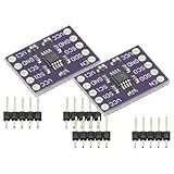
- 2Pcs I2C Module PCA9515A 2 Channel 2Bit I2C Repeater SMBus 400KHz Dual Bidirectional Repeater Module for Arduino
- Compatible with the IIC bus and System Management Bus (SMBus), the dual-way bidirectional IIC bus buffer repeater contains two identical bidirectional open-drain buffer circuits that can scale 2C and similar bus systems without compromising system performance.
- Since the 12C bus capacitance is limited to 400 pF, the number of devices and bus length are limited. With the PCA9515A, system designers can isolate the two halves of the bus to accommodate more 12C devices or longer wiring lengths. It can realize different level signal communication of 1IC devices on both sides of the buffer repeater, such as 5V and 3.3V signal level IIC communication.
- It can also match the communication rate of the I1C devices on both sides of the buffer repeater, such as 400KHz on one side and 100KHz on the other, but the maximum communication rate of the system will be slightly less than 100KHz because the buffer repeater has a delay. Two or more PCA951 5A cannot be cascaded. Devices For SDA and for SCL are open drain outputs.
Use isolation for the right problem
Isolation is appropriate where safety or ground-potential differences require electrically separate systems, not as a general fix for on-board crosstalk or a poor pull-up calculation. Check data rate, propagation delay, clock stretching, arbitration, common-mode limits, and startup behavior. Analog Devices’ AN-913 explains the bidirectional and isolation challenges of I²C.
Independent reader supportYour contribution helps us test, update, and keep practical guides available for everyone.Separate stuck buses and protocol behavior from noise
If SDA or SCL is stuck low
Identify which device is sinking the line before attempting recovery. A slave interrupted mid-transfer, a short, an unpowered peripheral, a translator, or reset sequencing can all produce a low line. Depending on the controller and target device, recovery may involve resetting the peripheral, power-cycling the slave, resetting the controller’s I²C block, or—if no other master can be active—releasing SDA and generating up to nine SCL pulses, followed by a STOP if the line can be released. This common technique is device- and controller-dependent, not a universal guarantee; follow the target’s recovery requirements.
If SCL stays low during a transaction
Check whether a device supports clock stretching and whether the controller handles it. A repeatable extended low period associated with a device operation may be legitimate. Distinguish it from a short glitch by inspecting the complete transaction and the analog SCL waveform.
If the high voltage is wrong
Verify each device’s I/O voltage range, the pull-up rail, translator topology, and power sequencing. A line pulled to a higher rail than a device permits can cause damage or intermittent behavior; a partially powered device may also load the bus.
Oscilloscope or logic analyzer?
An oscilloscope is the right tool to assess analog rise and fall times, ringing, overshoot, ground movement, and threshold crossings. A logic analyzer is useful for longer captures, transaction structure, ACK/NACK correlation, and firmware timing, but digital decoding alone cannot establish why the electrical waveform failed. Saleae notes that glitches around SCL edges can cause I²C decode failures in its I²C Analyzer guide.
Use a mixed-signal instrument or capture both instruments when you need analog detail and long protocol history. Probe close to the receiver: a test header can differ from the device pin. Long oscilloscope ground leads add inductance, and probe capacitance can alter a small bus. Use a short ground spring, a compensated probe, or an appropriate active or differential probe where the measurement requires it. If the scope is clean but the analyzer reports extra bits, check analyzer thresholds, sample rate, and ground reference. If the scope shows a disturbance that never approaches receiver thresholds, do not assume it caused the transaction failure.
Quick Recap
Quick troubleshooting checklist
- Confirm SDA and SCL pull-ups go to a safe voltage for every device.
- Find and account for all module pull-ups and their effective resistance.
- Check that both lines are high when idle and identify any device holding one low.
- Measure rise time at the receiver against the selected mode and device limits.
- Check VOL, fall time, overshoot, undershoot, and any threshold-crossing glitches.
- Use a short probe ground and compare the controller and remote-device waveforms.
- Inspect cable length, stubs, return path, connectors, and nearby switching signals.
- Test a lower bus speed and change only one variable at a time.
- Consider a buffer, switch, or isolation only when the topology or electrical requirement calls for it.
Product prices and availability are accurate as of the date/time indicated and are subject to change. Any price and availability information displayed on Amazon at the time of purchase will apply.
What’s actually slowing this PC down?
Pick the symptom - the matching free tool is one click away.

