
iTechGuides is reader-supported. When you buy through links on our site, we may earn an affiliate commission. As an Amazon Associate I earn from qualifying purchases. Learn more
The reliable way to detect laser damage is to measure the same defect or precisely registered region before and after processing, using matched optical, structural and spin measurements. Photoluminescence (PL) brightness is only a warning signal: laser exposure can change surface transmission, optical collection, charge-state balance or defect populations without destroying the diamond lattice. Pair PL spectra with an excited-state lifetime measurement, a structural check such as Raman spectroscopy (plus AFM or XRD when appropriate), and optically detected magnetic resonance (ODMR) or coherence data. Always include an untreated or otherwise matched control and report the sensitivity and sampled volume of every method.
What “damage” can mean in a diamond defect
“Damage” is not one measurement outcome. A laser can affect several layers of a diamond device, and they do not always change together. Define the failure you are testing before interpreting data.
Lattice or structural damage
This means a change in the diamond crystal itself, such as a new phase, defect-rich region, strain field or altered surface morphology. Raman spectroscopy can reveal phase- or lattice-related changes; atomic-force microscopy (AFM) measures surface topography; X-ray diffraction (XRD), or high-resolution XRD (HRXRD), can test structural parameters when the modified volume and geometry are large enough for the instrument. A measurement that looks unchanged at its available spatial resolution cannot rule out a nanoscale or highly localized alteration.
Quick wins for a faster PC:
Repair Windows errors before they cause bigger problemsFix Now →Fix the driver behind crashes, sound loss and screen glitchesFind Drivers →Clear out junk files and repair common Windows errorsFree Scan →Optical degradation
The defect may emit less light because the surface transmits less efficiently, the collection geometry has changed, or the local optical environment has been modified. That is an optical-quality problem even if the crystal lattice remains intact.
#1 Best Overall

- Wide Wavelength Range: 340-1000nm:Measure a broad spectrum of light, from UV to near-infrared, making it suitable for applications like lighting performance evaluation, color rendering analysis, and plant growth light testing.
- Compact & Ultra Lightweight Design:Engineered with NOSP material, this ultra-portable spectrometer measures just 47x28x25mm and weighs only 23g, offering excellent portability for fieldwork or on-the-go testing.
- Compatible with Android Devices(iOS not supported):Easily connect to Android smartphones using a USB Type-C port and dedicated mobile app.This wired connection provides stable, real-time light measurement capabilities for quick and efficient analysis.
- PC Software with One-Click Reporting:Analyze and save data effortlessly.The PC platform supports exporting measurement results in PDF format for professional reporting, ideal for researchers and lighting professionals.
- Versatile Applications Across Industries:Designed for various uses including indoor/commercial lighting evaluation,plant factory,OLED lighting tests,laboratory research,and even water or beverage analysis.
Defect loss or charge conversion
Laser exposure can remove, create, move or reconfigure color centers. For nitrogen-vacancy (NV) centers, the balance between negatively charged NV− and neutral NV0 can shift. Emission associated with NVH-related defects may also change. A lower NV− peak is therefore not automatically proof that the center was destroyed.
Spin-performance loss
A defect can retain optical emission while its ODMR contrast, resonance position, linewidth or coherence time changes. Conversely, spin behavior can remain stable even when a localized structural change exists. Spin degradation and lattice damage are related questions, not interchangeable diagnoses.
Set a defensible before-and-after experiment
The strongest test is a co-registered comparison: locate the same defect or written region before processing, repeat the measurement after processing, and compare it with an untreated nearby region or a matched sample. Keep the optical power, excitation wavelength, focus, collection path, detector settings, magnetic field, temperature and microwave conditions the same unless a deliberate change is part of the experiment.
Recommended Free Tools
Record the processing variables alongside the measurements. At minimum, log wavelength, pulse duration, pulse energy or fluence, number of pulses, repetition conditions, focus and spot size, scan speed or dwell time, and whether the beam was stationary or scanned. Also identify the diamond type, nitrogen and other defect background, surface preparation, sample geometry and the volume that the probe actually samples. These details determine whether two apparently similar results are genuinely comparable.
Step-by-step diagnostic workflow
1. Mark and document the region
- Capture a registration image. Use the same microscope coordinates, fiducial marks or surface features that will let you return to the defect after processing. Save a map rather than relying on a stage coordinate alone.
- Measure an untreated reference. Choose a nearby region with similar depth, crystal orientation and background defects. If the process covers a large area, prepare a matched unprocessed sample as well.
- Write down the process history. Include all pulse and fluence information, not just “laser power.” A change attributed to damage may instead result from a different dose or focal volume.
Registration errors are a common false positive. If the post-process measurement samples a neighboring defect or a different depth, an apparent intensity or spin change has no clear causal link to the laser.
Rank #2

- VERSATILE APPLICATIONS || Whether you're studying light sources, exploring color spectra, or conducting in-depth analyses, this spectroscope provides the functionality you need for accurate measurements. It is versatile enough to measure spectra emitted from charged gas tubes, flame tests, and during basic astronomy applications
- INNOVATIVE DESIGN FOR LEGIBLE READINGS || Features a thoughtful design that securely holds the diffraction grating and scale - no more taping the grating and scale to the body. This ensures clear and legible readings, eliminating the frustration of unreliable or blurry measurements
- WIDE MEASUREMENT RANGE || With the ability to measure wavelengths from 400.0 to 700.0nm, this spectroscope offers a comprehensive range for detailed examination
- DIFFRACTION GRATING || The spectroscope features a diffraction grating with 500 lines/mm, ensuring optimal performance and high-resolution spectra. This premium grating enhances the accuracy and detail of your measurements, allowing you to observe and analyze light sources with greater precision and clarity
- PRECISE & ACCURATE RESULTS || Achieve precision measurement with an accuracy of +/- 5.0nm. This spectroscope delivers reliable and accurate results, enabling you to make confident conclusions and draw valuable insights from your observations. Whether you're conducting scientific research, studying light properties, or performing experiments, this spectroscope is a reliable tool you can trust
2. Map PL intensity and spectrum under identical settings
Start with a confocal or equivalent PL map of both the processed and control areas. Use the same excitation power, integration time, objective, focus, detector gain and spectral response correction. Record the complete spectrum, not only integrated counts. For NV material, separate the NV− and NV0 signatures and note any change in NVH-related emission.
A brightness change is an investigation trigger. A 2026 multipulse-laser study explicitly reported: Laser irradiation affects transmittance of diamond surface and NV center brightness.
That observation does not identify whether the cause is lattice damage, altered transmission, charge conversion, a changed defect population or collection drift. Check the untreated region in the same run to distinguish a sample-wide optical change from a local one.
The Tool Desk
Outbyte Driver Updater FREEScan for outdated or missing drivers - takes under a minuteDriver Scan →Outbyte PC Repair FREEClear out junk files and repair common Windows errorsFree Scan →3. Add an excited-state lifetime or quenching measurement
Measure the PL decay with time-correlated single-photon counting (TCSPC) when available. Compare the excited-state lifetime of the same defect before and after processing, and compare both NV− and NV0 channels where the spectrum permits. A change in counts with a stable lifetime points toward excitation, transmission, collection or population effects; a lifetime change indicates that the radiative or non-radiative environment has changed.
Lifetime and intensity together are more informative than intensity alone. Ensure that detector timing, instrument-response correction, excitation power and fitting procedure are held constant. Report the uncertainty and whether the decay was measured from a single center, an ensemble or a spatial average.
4. Check crystal and surface structure
Use Raman spectroscopy to look for phase or lattice-related signatures at the processed site and the control. Pair it with AFM if surface roughness, pits, swelling or a localized topographic feature is plausible. Use XRD or HRXRD only when the modified volume, orientation and geometry provide enough signal for those methods.
Rank #3

- Specifications: Full-spectrum spectrometer measuring 380ñ780nm, CMOS sensor, 1,600ñ40,000K CCT range, 1ñ200,000lx ambient & 20ñ20,500lx∑s flash, CRI, TLCI, TLMF, TM-30-18 & SSI metrics, 4.3" touchscreen LCD.
- Advanced Color Metrics: Displays CRI, TLCI, TLMF, TM-30-18 and SSI values for comprehensive evaluation of spectral similarity and color rendering performance across LED, HMI, fluorescent and flash sources.
- Precision LED Matching: Provides CIE 1931 x,y chromaticity coordinates with hue and saturation analysis, enabling accurate matching of RGB, RGBW and RGBAW LED fixtures in seconds.
- Wide Measurement Capability: Covers broad color temperature and illuminance ranges for both ambient and flash applications, supporting demanding cinematography and commercial photography workflows.
- Professional Ergonomics: 270∞ swivel head, dark calibration without cap, large 4.3" color touchscreen, and customizable interface streamline operation in studio and on-location environments.
A recent nanosecond-laser irradiation study found a localized modification while Raman, AFM and XRD indicated preserved crystal quality under its particular process and sample conditions. That result shows why several probes are useful, but it is not a universal guarantee: a structural change smaller than the probe’s spatial resolution can remain invisible. Report the laser-site registration, lateral and depth resolution, sampling area and detection limit.
Do these 3 things before closing this tab:
1Fix the driver behind crashes, sound loss and screen glitches2Repair Windows errors before they cause bigger problems3Scan for outdated or missing drivers - takes under a minute5. Test spin function with ODMR and, when relevant, coherence
Record ODMR spectra under the same optical power, magnetic field, temperature, microwave frequency sweep, microwave power and collection settings used for the baseline. Compare resonance frequency, linewidth, contrast and any splitting or strain-related features. If the application depends on coherence, measure a relevant quantity such as T2 with the same pulse sequence and timing.
ODMR confirms that a spin-active population is responding; it does not identify the physical mechanism behind a changed signal. A contrast loss may reflect charge conversion, optical background, microwave coupling or true spin-environment degradation. Conversely, an unchanged ODMR or T2 does not exclude a small structural modification.
6. Analyze controls and sensitivity before assigning damage
Process the before/after and control data with the same background subtraction, spectral calibration and registration procedure. State the smallest change each technique could have detected and the volume or surface area it sampled. “No difference” means no difference above those limits, not proof that no nanoscale change occurred.
How to read combinations of results
| Observed result | What it supports | What it does not prove |
|---|---|---|
| PL intensity changes, while lifetime and spectrum remain stable | A change in excitation, collection, transmission or defect population is plausible; inspect the control and surface transmission. | Structural damage by itself. |
| NV−/NV0 balance or NVH-related emission changes | Defect-population or charge-state reconfiguration is plausible. | That the original quantum defect was lost. |
| Raman, AFM or XRD changes co-located with the laser site | Structural or surface modification is supported. | That the NV’s spin function is necessarily degraded. |
| ODMR contrast, resonance behavior or T2 degrades | Spin performance changed under the measured conditions. | The specific damage mechanism or lattice damage without structural evidence. |
| No detectable difference | No change above the tested methods’ sensitivity and spatial resolution. | Absence of all nanoscale or highly localized damage. |
Why PL brightness alone gives ambiguous answers
Integrated PL counts combine several factors: the number of emitting centers, their charge states, excitation efficiency, radiative and non-radiative rates, surface transmission and the collection path. Laser processing can alter any of these. For example, a center may become brighter because a laser creates or activates additional NV centers, while a damaged surface may reduce the light reaching the detector. A charge conversion from NV− to NV0 can lower the signal in one spectral window while leaving total emission less changed.
Free tools Windows power users keep installed
One-click scans. No signup required.
Rank #4

- Wireless bluetooth connection, the sensor can detaches from screen body. Wavelength range of Spectrometer PPFD Meter PAR Quantum Meter is 350 to 800 nm
- PPFD PAR Meter for grow light testing, lux, cct, cri, ppfd, par..etc.
- Light Measurement Meter measuring range (color temp) 1,000 to 100,000K (Illuminance) 10 to 200,000lx, FWHM 4nm. wavelength accuracy of ppfd light meter is ±1nm.
- PPFD spectrometer with screen, that you can test and save data in device, then you can export excel file, also can use pc software to print reports.(works on windows system)
- Bring Anywhere: From squeezing into tight places to keeping your load light, you can bring spectrometer wherever you need to. Fits easily into a work bag or large pocket and barely adds any weight. It's the ultimate in light-metering convenience!
Use the spectrum to separate these possibilities, then use lifetime data to test for quenching. If the spectrum and lifetime are stable but counts fall only at the processed site, inspect focus, surface transmission, contamination and collection geometry before calling it defect damage. If the charge-state balance shifts, describe it as a charge or population change unless independent structural and spin evidence supports a stronger conclusion.
What each structural method can and cannot establish
Raman spectroscopy
Raman is useful for detecting phase- or lattice-related spectral changes at the laser location. It samples a finite optical volume, so a narrow damaged filament, a buried point defect or a change below its spatial resolution may not produce a resolvable difference. Compare identical polarization, focus, spectral calibration and acquisition time.
Atomic-force microscopy
AFM tests the surface directly. It can reveal pits, ridges, roughness or swelling that an optical spectrum cannot. It cannot by itself determine whether a buried NV center has lost spin coherence, and a smooth surface does not prove that the subsurface lattice is unchanged.
XRD and HRXRD
Diffraction can test crystal parameters and strain when the affected volume and orientation provide sufficient signal. A microscopic modification may be diluted by the surrounding bulk crystal. State the beam size, geometry and volume fraction that were actually interrogated.
Crashes, No Sound, or Screen Glitches?
Random freezes, missing sound and display glitches usually trace back to one bad driver. Find and replace yours safely.Free scan · under a minutePC Slower Than It Used to Be?
A free scan shows the junk files, broken settings and background clutter dragging Windows down - then fixes them in one click.Free scan · Windows 10 & 11What spin measurements add
ODMR links the optical signal to a measurable spin transition. Compare resonance frequency, linewidth and contrast, not just whether a peak is visible. A resonance shift can indicate a changed local field or strain, but the shift alone does not prove a damaged lattice; temperature, magnetic-field alignment and charge-state changes can also matter.
Best Value
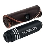
- COMPACT AND PORTABLE: Crafted to be travel-friendly, this pocket-sized Spectroscope device is incredibly small and portable. Whether you're exploring gem markets, embarking on vacations, or attending trade shows, it easily fits in your pocket or bag, making it convenient to carry around
- UNPARALLELED CONSTRUCTION: The Pocket-Sized Diffraction Spectroscope is meticulously crafted from aircraft aluminum, ensuring durability and longevity. Combined with the finest optics available, this tool guarantees exceptional performance and accurate results
- UNLEASH ITS POTENTIAL: Equipped with a high-quality grating, our spectrometer enables you to delve into the world of gemology with confidence. Identify gemstones swiftly and precisely, including the "diamond stimulants" YAG and Cubic Zirconia, which serve as valuable aids in detecting iron and chromium
- ELEVATE YOUR GEMSTONE IDENTIFICATION: With the Pocket-Sized Grating Gemological Spectroscope , you gain an indispensable tool that empowers you to unlock the secrets of gemstones effortlessly. Enhance your gemological expertise and make informed decisions with this exceptional instrument by your side
- EASY TO USE: The Pocket-Sized Spectrometer wavelengths that are absorbed by the stone are seen in the spectroscope as verticle black lines in the spectrum. Each stone has a unique absorption spectrum (like a fingerprint of the stone) When identifying a stone we look for a spectrum that is characteristic for that stone
Coherence measurements address function directly. A 2020 study of radiation damage found no coherence-time change at its tested dose in its specified type IIa diamond sample. That finding demonstrates that additional vacancy-related damage need not always reduce NV coherence. It should be treated as a condition-specific result, not a pass/fail rule for every laser process, diamond type or dose.
Independent reader supportYour contribution helps us test, update, and keep practical guides available for everyone.How to compare two laser processes or samples
When deciding which process is less damaging, compare the same measurement axes rather than brightness alone.
| Axis | Record for each condition | Why it matters |
|---|---|---|
| Optical output | Co-registered PL intensity, full spectrum, NV−/NV0 balance and NVH-related features. | Separates brightness changes from charge or population changes. |
| Quenching | Lifetime or decay behavior, with uncertainty and acquisition settings. | Tests whether the emitting state’s radiative environment changed. |
| Structure and surface | Raman, AFM and XRD/HRXRD results plus lateral and depth resolution. | Prevents a bulk measurement from being interpreted as proof about a nanoscale site. |
| Spin function | ODMR contrast, resonance and linewidth; T2 or another relevant coherence metric. | Shows whether the defect still performs its intended spin function. |
| Laser dose | Wavelength, pulse duration, fluence or energy, pulse count and focusing geometry. | Different dose regimes can produce opposite defect responses. |
| Sample and measurement context | Diamond type, nitrogen/defect background, geometry, temperature, field, optical power and microwave conditions. | Limits how broadly a result can be generalized. |
There is no single universal numerical damage threshold established across these variables. A process that is benign for one type IIa sample at one wavelength and pulse history may behave differently in another diamond or at another depth.
Quantitative figures that need careful qualification
A 2026 Elsevier study of laser-generated NV centers reported an absorption cross-section of about 5.5 × 10⁻¹⁷ cm2 and a room-temperature T2 of 64 μs for the single NV center and conditions it studied. These are properties reported for that experiment, not a laser-damage threshold or a universal acceptance criterion. Do not use either number as a pass/fail limit for a different defect, pulse regime or sample.
Likewise, the 2026 nanosecond-laser study’s preserved Raman, AFM and XRD crystal-quality indicators apply to its process and specimen. They support the narrower statement that localized modification can occur without a detectable loss of crystal quality under those tested conditions.
Troubleshooting misleading results
The post-process PL map is dimmer everywhere
- Recheck focus, objective alignment, detector gain and excitation power with a stable reference sample.
- Inspect the surface for contamination or altered transmission.
- Compare the untreated region measured in the same session. If it also changed, suspect instrument drift or a sample-wide optical effect before local damage.
Only one charge-state peak changed
- Verify spectral calibration and background subtraction.
- Report NV− and NV0 separately rather than folding them into one brightness value.
- Use lifetime and ODMR data to determine whether the center remains optically and spin active.
Raman appears unchanged but ODMR degraded
- Check that optical power, magnetic field, temperature and microwave coupling match the baseline.
- Consider charge conversion, increased optical background or a changed local spin environment.
- Do not label it lattice damage without independent structural evidence.
ODMR is unchanged but the surface looks modified
- Confirm that the same defect was addressed and that the modified feature lies within the optical path.
- Measure lifetime and PL spectrum for quenching or charge changes.
- Recognize that preserved spin performance does not rule out a localized surface or lattice change.
Every method reports “no change”
- State the detection limit, spatial resolution and sampled volume for each method.
- Check whether the laser spot or depth is smaller than the probe’s effective resolution.
- Use a more localized measurement or a higher-sensitivity method if the application requires ruling out nanoscale damage.
How to report a damage assessment
A reproducible report should let another laboratory distinguish a real defect response from a measurement artifact. Include:
- Diamond type, orientation, nitrogen concentration or relevant defect background, surface preparation and geometry.
- Laser wavelength, pulse duration, pulse energy or fluence, pulse count, repetition conditions, focus, spot size and scan or dwell details.
- Before-and-after registration method and the location and size of untreated controls.
- PL excitation, collection, detector and integration settings; complete spectra and charge-state analysis.
- Lifetime instrument, timing calibration, fitting method and uncertainty.
- Raman, AFM and XRD/HRXRD geometry, probe resolution and detection limits.
- ODMR optical power, magnetic field, temperature, microwave conditions, resonance metrics and coherence sequence.
- The exact region and depth sampled by every technique, including any mismatch between a bulk probe and a nanoscale processed volume.
Decision rule
Call laser processing damaging only when the evidence supports a defined failure mode. A co-located structural change supports structural modification; a reproducible lifetime or charge-state change supports altered defect photophysics; and degraded ODMR or coherence supports impaired spin function under the measured conditions. A PL change alone is a reason to investigate, not a diagnosis. The most defensible conclusion combines co-registered before-and-after data, matched controls, at least one optical-lifetime or spectral discriminator, a structural probe suited to the affected scale, and a spin measurement when the defect’s quantum function matters.
Quick Recap
Product prices and availability are accurate as of the date/time indicated and are subject to change. Any price and availability information displayed on Amazon at the time of purchase will apply.

