
The Tool Desk
Outbyte Driver Updater FREEFix the driver behind crashes, sound loss and screen glitchesFind Drivers →Outbyte PC Repair FREERepair Windows errors before they cause bigger problemsFix Now →iTechGuides is reader-supported. When you buy through links on our site, we may earn an affiliate commission. As an Amazon Associate I earn from qualifying purchases. Learn more
AI chips are designed around the computations and data movement a workload requires, built through repeated semiconductor manufacturing steps, and packaged into systems that supply memory, power, cooling, networking, and software. Their real-world capability depends on that whole system—not just the accelerator’s advertised arithmetic throughput.
What an AI chip does—and why it is part of a larger system
An AI accelerator is a processor designed to speed up operations used by machine-learning models. It may be a GPU, a custom application-specific integrated circuit (ASIC), or another specialized processor. The chip performs calculations, but useful work depends on getting model data to it, coordinating it with other processors, and keeping the system within power and temperature limits.
That is why “How fast is the chip?” is not enough to evaluate one. A model may be limited by compute, memory capacity, memory bandwidth, communication among accelerators, software support, or the ability to power and cool the installed equipment. A fast chip that cannot keep its compute units supplied with data—or that is difficult to program for the target workload—may not produce the best result for that job.
Free tools Windows power users keep installed
One-click scans. No signup required.
Training and inference also place different demands on the system. Training adjusts model parameters over repeated passes through data and may involve large-scale coordination among accelerators. Inference runs a trained model to produce an output; it can involve many small requests, large batches, or low-latency responses. These patterns influence which operations, data types, memory arrangements, and links a design should prioritize.
#1 Best Overall

- ATTENTION BUYERS: EXPORTING this item outside the U.S. requires strict compliance with the Bureau of Industry and Security (BIS) U.S. Export Administration Regulations (EAR). Non-compliance carries fines up to $1 MILLION PER VIOLATION AND UP TO 20 YEARS IMPRISONMENT for both the buyer and seller. To uphold our regulatory obligations, we strictly follow BIS "Know Your Customer" guidance by screening each order and immediately aborting transactions showing unresolved regulatory red flags. ***
- [Double-Flow-Through Design] The RTX PRO 6000 Blackwell features a double-flow-through cooling design, optimizing efficiency and airflow to sustain peak performance under 600W power loads. | [5th Gen Tensor Cores] Deliver up to 3X the performance of the previous generation and support for FP4 precision for faster AI model processing times with reduced memory usage, enabling local fine-tuning of LLMs and generative AI | [4th Gen Ray Tracing Cores] Double the ray-triangle intersection rate of the previous generation to create photoreal, physically accurate scenes and immersive 3D designs with RTX Mega Geometry, which enables up to 100X more ray-traced triangles.
- [PCIe Gen 5] Support for PCIe Gen 5 provides double the bandwidth of PCIe Gen 4, improving data-transfer speeds from CPU memory and unlocking faster performance for data-intensive tasks like AI, data science, and 3D modeling. | [GDDR7 Memory] With 96 GB of GPU memory and 1.8 TB ps bandwidth, it can tackle massive 3D and AI projects, fine-tune AI models locally, explore large-scale VR environments, and drive larger multi-app workflows.
- [DisplayPort 2.1] Achieve unparalleled visual clarity and performance, driving high resolution displays at up to 8K at 240 Hz and 16K at 60 Hz. Increased bandwidth enables seamless multi-monitor setups while HDR and higher color depth support ensures superior color accuracy for precision work, such as video editing, 3D design, and live broadcasting.
- [NVIDIA Blackwell Streaming Multiprocessor] The new SM features increased processing throughput, and new neural shaders that integrate neural networks inside of programmable shaders | DLSS 4: Multi Frame Generation ensures ultra-smooth frame pacing for lifelike simulations. | [Universal MIG] Divide a single RTX PRO 6000 Blackwell into multiple isolated instances, each with dedicated resources, allowing for concurrent execution of multiple workloads, optimized GPU utilization, and secure isolation of different applications or users. [WARRANTY] 3 YR Manufacturer's Warranty. Bulk OEM Packaging. Retail Packaging is NOT included.
How workload requirements shape chip architecture
Choose compute, data formats, and memory for the target work
Design begins with a target: the models and operations the chip is expected to run, how much performance is needed, and the limits imposed by cost, power, and deployment scale. Architects choose compute units and supported numerical formats, then decide how to organize on-chip memory and access to external memory. The aim is not simply to maximize arithmetic units; it is to keep them useful by moving the right data to the right place at the right time.
Memory capacity determines how much data can be held close to a processor, while bandwidth describes how quickly that data can be transferred. If a model or its working data does not fit in fast memory, it may need transfers from elsewhere in the system. Those transfers can constrain performance even when the chip’s arithmetic hardware has headroom. The same issue arises across chips: a multi-accelerator job needs efficient communication as well as fast individual processors.
Design the links as well as the processors
Interconnects carry data between components, from processors within a package to accelerators across a server or rack. NVIDIA describes its NVLink-C2C as providing coherent, high-bandwidth transfers between processors. The company also says interconnect layout affects performance, power efficiency, reliability, and fabrication yield—an illustration of how physical layout and system communication are intertwined rather than separate finishing details.
Quick wins for a faster PC:
Scan for outdated or missing drivers - takes under a minuteDriver Scan →Repair Windows errors before they cause bigger problemsFix Now →Fix the driver behind crashes, sound loss and screen glitchesFind Drivers →NVIDIA claims NVLink-C2C can deliver up to 6× the energy efficiency and 3.5× the area efficiency of a PCIe Gen 6 PHY in its chips. These are NVIDIA’s stated comparisons, not independent measurements or a guarantee for every workload or system. The broader design point is that a link’s bandwidth, power use, physical footprint, and implementation all matter when multiple components must cooperate.
Blackwell as a multi-die example
NVIDIA describes its Blackwell GPU architecture as having 208 billion transistors and using a custom TSMC 4NP process. It combines two reticle-limited dies connected by a 10 TB/s chip-to-chip interconnect. These are manufacturer-published specifications for that architecture, not independent benchmark results.
A reticle limits the maximum area that can be patterned in one exposure, so a design that exceeds that limit may use more than one die. In Blackwell, the two dies are joined with a high-bandwidth connection so they can function as one GPU. The example shows why the division of a design into dies, the link between them, and the package that holds them are architectural choices—not just manufacturing trivia.
How a design becomes a silicon wafer
Verify the design before manufacturing
Before fabrication, engineers develop and verify the chip design. Verification checks that the design behaves as intended under relevant conditions; it is essential because errors discovered after wafers are made can be expensive to correct. Design tools also support choices about physical layout and how the intended circuits can be built.
NVIDIA’s semiconductor overview describes computational lithography as a way to optimize photomasks to counteract patterning issues. A photomask carries a pattern used during lithography, the process that transfers circuit features onto a wafer. Computational tools help account for the fact that the printed result can differ from an idealized drawing at extremely small scales. This is one example of software supporting both chip design and the manufacturing process.
Rank #2
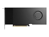
- Professional GPU with Blackwell Architecture
- Blackwell Architecture
- 24GB GDDR7 with PCIe 5.0 & Ray Tracing
- AI Workstation
Repeat processing and patterning on the wafer
A foundry fabricates chips by processing a silicon wafer through many stages. At a high level, materials are deposited or otherwise formed in layers, patterns are transferred, and etching and other processes create device structures and wiring. The cycle repeats to build the complex arrangement of transistors and connections. The exact recipe varies by process and is far more detailed than this overview.
NVIDIA’s account of Blackwell production names layering, patterning, etching, and dicing. After wafer processing, dies are tested and the wafer is cut into individual pieces. A die that passes the relevant checks can proceed to packaging; a wafer is not a finished data-center accelerator by itself.
Why packaging, memory, and interconnect matter
Packaging brings one or more dies together with connections to memory and the rest of the system. It can make short, high-bandwidth links between components possible, while also addressing physical and thermal constraints. The details differ by design: a two-die GPU and a processor with attached high-bandwidth memory are examples of choices made for particular architectures, not a universal packaging formula.
Do these 3 things before closing this tab:
1Clear out junk files and repair common Windows errors2Scan for outdated or missing drivers - takes under a minute3Repair Windows errors before they cause bigger problemsGoogle says its Ironwood TPU uses eight HBM3E memory stacks per chip, with 192 GiB of capacity and peak bandwidth of 7.4 TB/s. These are Google-published specifications for that TPU generation, described in 2025. High-bandwidth memory can supply data at substantial rates, while its capacity determines how much can be held in those memory stacks. Neither figure alone establishes how quickly a complete application will run; the result also depends on the workload, software, and the rest of the system.
Packaging and interconnect are closely related. Components placed together can use short links, but the module still has to connect to host processors, other accelerators, and networking. Designers must balance data movement, power, reliability, manufacturing constraints, and heat. This is why a chip’s published specifications need to be read as part of its platform rather than as a complete description of performance.
How accelerators become a data-center system
Servers and racks provide the operating environment
Once packaged, accelerators are installed in servers with host CPUs, memory, storage, networking, and power delivery. Servers are then connected into racks and data-center networks. Power systems must deliver energy to the equipment, and cooling must remove the heat that operation produces. The more accelerators and links a system contains, the more important it becomes to design and operate these supporting systems as part of the platform.
Software is another essential layer. Drivers, compilers, libraries, and model frameworks help map an application onto a particular accelerator and distribute work across multiple devices. A system’s software support and the skills needed to operate it can therefore affect whether it is practical for a given workload, even if its hardware specifications appear attractive.
Rack-scale and pod-scale approaches
NVIDIA describes GB200 NVL72 as a rack-scale design containing 36 GB200 Grace Blackwell Superchips, with 36 Grace CPUs and 72 Blackwell GPUs. That is a vendor-published system specification, not an independent performance measurement. The figures describe a coordinated rack-scale platform rather than an individual GPU.
Rank #3
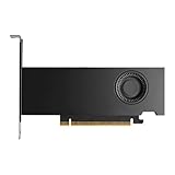
- Form Factor: Plug-in Card
- Cooler Type: Active Cooler
- Maximum Power Consumption: 70W
- Length: 6.6
- Height: 2.7
Google describes Ironwood TPU pods and the ability to scale multiple superpods through a data-center network. This is a different system approach from the cited NVIDIA rack configuration. The useful comparison is architectural: how each platform organizes its processors and memory, connects devices within a system and across systems, and provides software access. The available specifications do not establish a controlled, current GPU-versus-TPU performance winner.
For a real deployment decision, compare systems against the actual application. Relevant questions include whether the workload is training or inference; which software and model tools it requires; how much memory it needs and how quickly data must move; how the accelerators scale together; and whether the organization can provide or access the needed power, cooling, networking, and operational expertise.
Independent reader supportYour contribution helps us test, update, and keep practical guides available for everyone.What happens when an AI workload runs
At a simplified level, software breaks a model’s work into operations that the accelerator can execute. The chip performs those operations using its compute units, draws model parameters and intermediate data from memory, and exchanges information with other processors when the job is distributed. The server and data-center network coordinate data and results, while power and cooling keep the equipment within operating limits.
Training may distribute computation across many accelerators, making communication and coordination important alongside raw compute. Inference can be deployed to serve requests using a trained model; its system needs depend on the required response time, request volume, and model size. The same hardware can have different value in different jobs because utilization, data movement, software, and deployment constraints vary.
The original Google TPU provides a historical example of a purpose-built inference accelerator. A 2017 paper by Google researchers describes a custom ASIC deployed in Google data centers since 2015 for neural-network inference. It states: “The heart of the TPU is a 65,536 8-bit MAC matrix multiply unit that offers a peak throughput of 92 TeraOps/second (TOPS) and a large (28 MiB) software-managed on-chip memory.” Those figures refer to the first-generation TPU and its reported peak throughput, not to current TPU hardware or a comparable benchmark against modern accelerators.
How to interpret AI-chip specifications
Published specifications help explain design choices, but figures from different generations and vendors cannot be treated as a head-to-head result unless they use comparable workloads, measurement methods, and system conditions. For example, the first TPU paper’s 92 TOPS is a historical peak figure for a specific 8-bit device, while Ironwood’s 7.4 TB/s figure is Google’s stated peak memory bandwidth for a later TPU generation. They measure different things and are not a performance comparison.
- Compute: Check the operation type and numerical format associated with a throughput figure. A peak rate is not the same as achieved application performance.
- Memory: Look at both capacity and bandwidth, then consider whether the workload’s model and intermediate data fit the system’s memory hierarchy.
- Interconnect: Identify the links within a package, between accelerators in a server or rack, and across the data-center network. A number for one type of link does not describe the others.
- Software: Confirm that the frameworks, libraries, and model operations needed by the workload are supported and that the team can use them effectively.
- System constraints: Account for power delivery, cooling, networking, and the scale of infrastructure required to operate the accelerators.
- Access model: Distinguish infrastructure an organization owns and operates from accelerators accessed as a cloud service. A hardware architecture description does not establish current cloud regions, configurations, or commercial terms.
For current GPUs and TPUs, the cited platform descriptions provide architecture and vendor specifications, not controlled cross-vendor benchmarks. A defensible selection requires workload-specific measurements on the configurations and software the intended deployment will actually use.
Recommended Free Tools
Quick Recap
Product prices and availability are accurate as of the date/time indicated and are subject to change. Any price and availability information displayed on Amazon at the time of purchase will apply.

