
Recommended Free Tools
iTechGuides is reader-supported. When you buy through links on our site, we may earn an affiliate commission. As an Amazon Associate I earn from qualifying purchases. Learn more
There is no universal winner. FD-SOI is a strong candidate when a design needs very low power, always-on operation, RF or analog integration, or adaptive body-bias control. FinFET is a strong candidate when logic density and compute-intensive performance dominate. The right choice depends on the specific foundry platform, workload, voltage, libraries, IP, manufacturing plan, and total project cost—not on the process label alone.
What is the practical difference between FD-SOI and FinFET?
FD-SOI, or fully depleted silicon-on-insulator, is a transistor technology built on a thin silicon layer separated from the substrate by a buried insulating layer. FinFET uses a three-dimensional fin-shaped channel with gate control around multiple sides of the fin. Those structures affect how a process platform balances power, performance, density, and design flexibility. The labels alone do not specify a chip’s results: node, libraries, circuit design, voltage, workload, and the foundry’s available options all matter.
For a low-power design, FD-SOI’s most distinctive lever is body biasing. A designer can apply a bias to the body of the transistor to alter its behavior, and an adaptive scheme can adjust that bias as operating conditions or performance needs change. GlobalFoundries describes forward body biasing in its FDX platform as a way to tune performance and energy efficiency dynamically. A real implementation depends on support in the process, design libraries, IP, and control circuitry; it is not a free performance or power improvement that can be assumed from the process name.
FinFET’s strongest general case is logic density. GlobalFoundries positions its FinFET offering for maximum logic density and compute-intensive designs. That can be important when a chip’s performance target, logic area, or integration needs make density a decisive factor. It does not, by itself, prove that every FinFET implementation will beat every FD-SOI design on speed, power, or cost.
#1 Best Overall
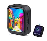
- ESP32-S3R8 Processor--- Equipped with ESP32-S3R8 Xtensa 32-bit LX7 dual-core processor, up to 240MHz main frequency. Supports 2.4GHz W-i-F-i (802.11 b/g/n) and Blue--tooth 5 (LE), with onboard antenna. Built in 512KB of SRAM and 384KB ROM, with onboard 8MB PSRAM and an external 16MB Flash memory.
- AMOLED Touch Screen--- Onboard 1.8inch AMOLED display for clear color picture display, 368 x 448 resolution, 16.7M color, 178° wide viewing angle. Compared to those traditional LCD displays, the AMOLED screen features precise light-control capability, representing more delicate colors, more picture details, and more vivid video image.
- Onboard Audio Codec---Supports high-quality audio processing, providing clear and high-quality audio input and output. Supports Offline Speech recognition and AI Speech Interaction---Allows access to online large model platforms to support more AI application scenarios.
- For Various Smart Devices---Suitable For Various Smart Devices Development, Can Realize Human-Computer Interaction Function. Supports installing ba|tte|ry inside the case for independent operation. (Note: this version doesn't include ba|tte|ry ) Dedicated Black Case---with removable back cover for easy embedded into the projects and DIY design.
- Sensor and Chip---Onboard QMI8658 6-axis IMU (3-axis accelerometer and 3-axis gyroscope) for detecting motion gesture, counting steps, etc. Built-in SH8601 display driver and FT3168 capacitive touch chip, using QSPI and I2C communication respectively, effectively saving the IO resources.
Both descriptions are platform positioning, not a controlled, matched benchmark. A meaningful comparison puts two actual foundry offerings against the same workload, performance target, voltage range, design scope, and production assumptions.
When is FD-SOI the better candidate?
Start with FD-SOI when power management is a central architectural requirement and the selected platform offers features that directly support it. A design that spends much of its life in a standby or always-on state, or one that must move between low-power and higher-performance operating modes, may be able to use adaptive body biasing to tune behavior for its current needs. Whether that produces a worthwhile system benefit must be demonstrated in the design and its power-management scheme.
FD-SOI may also be a good fit when a single chip combines digital logic with RF or analog functions, embedded memory, high-voltage I/O, or automotive features. GlobalFoundries describes its FDX platform as combining digital, analog, and RF integration, adaptive body biasing, embedded non-volatile memory options, and automotive and high-voltage features. Those are platform-specific options to verify in the relevant process design kit (PDK), not universal properties of every FD-SOI process.
Free tools Windows power users keep installed
One-click scans. No signup required.
CEA-Leti identifies communications—including 5G and sub-6 GHz applications—automotive radar, lidar and microcontrollers, smart devices and IoT, embedded AI components, and space components as FD-SOI application areas. It also describes back-biasing as a way to adjust performance and power consumption to an application’s needs. These examples establish that FD-SOI is used across varied application categories; they do not establish that a particular foundry, node, IP block, or production slot is available to every project.
Rank #2

- 2.4GHz Dual Mode WiFi + Bluetooth Development Board
- Support LWIP protocol, Freertos
- SupportThree Modes: AP, STA, and AP+STA
- Ultra-Low power consumption, Compatible with Arduino IDE
- ESP32 is a safe, reliable, and scalable to a variety of applications
FD-SOI is worth evaluating when
- Power in both active and standby modes is a major constraint, and workload behavior offers opportunities for bias or voltage management.
- The platform’s supported body-bias range, libraries, and IP match the intended control strategy.
- RF, analog, embedded memory, high-voltage I/O, or automotive features need to coexist with digital logic, and the specific platform supports those requirements.
- The design’s performance and area targets can be met by the candidate FD-SOI node and its available libraries.
- The design team can obtain a suitable PDK, qualified IP, EDA flow, foundry capacity, and schedule.
GlobalFoundries says FDX is designed for system-level cost efficiency through lower power, higher integration, and reduced design complexity. Treat that as the platform’s stated design intent, not a promise that every project will have a lower total cost. Integration may simplify a system in some cases, but the project’s actual silicon, IP, design, qualification, and manufacturing costs must be assessed together.
When is FinFET the better candidate?
FinFET is the more natural candidate to investigate when the chip is compute-intensive and logic density is a primary constraint. A density advantage can matter if it helps fit more logic into a target die area, supports the needed compute capacity, or enables a desired level of integration. The practical question is not whether FinFET is generically “faster,” but whether the chosen FinFET platform, libraries, and implementation satisfy the design’s performance and power targets at an acceptable area and project cost.
GlobalFoundries characterizes its FinFET process as designed for demanding high-performance and mission-critical processing. That characterization is vendor positioning, not an independent comparison against a particular FD-SOI chip. A team should verify the particular FinFET platform’s RF, analog, embedded-memory, and other feature support instead of assuming that all FinFET offerings have the same capabilities.
FinFET is worth evaluating when
- Compute throughput or logic density is more important than having body-bias flexibility as a central design lever.
- The candidate platform’s libraries can meet the required performance, area, and power targets under the actual workload.
- Any RF, analog, memory, I/O, safety, or mission requirements are supported by the exact process and its IP ecosystem.
- The foundry can supply the required PDK, qualified IP, design flow, capacity, and production schedule.
Do not presume an equivalent body-bias mechanism on a FinFET platform just because it is available in an FD-SOI offering. Compare the actual process options and design support offered by the candidate foundries.
Rank #3

- 2.4GHz Dual Mode WiFi + Bluetooth Development Board
- Support LWIP protocol, Freertos;ESP32 is a safe, reliable, and scalable to a variety of applications
- SupportThree Modes: AP, STA, and AP+STA
- Ultra-Low power consumption, Compatible with Arduino IDE
- 1PCS 30Pin ESP32 Development Board 2.4GHz WiFi Dual Cores Microcontroller Integrated with Antenna RF Low Noise Amplifiers Filters
Compare candidate platforms against the same design requirements
Use a concrete design brief rather than asking which technology wins in the abstract. The table below turns the key differences into questions for a foundry and design team. The answers should be specific to named platforms and supported by PDK data, IP documentation, design estimates, and current commercial terms.
| Decision area | Questions for an FD-SOI platform | Questions for a FinFET platform |
|---|---|---|
| Active and standby power | Does the workload benefit from low operating voltage, the platform’s leakage behavior, or body-bias tuning? What do the design estimates show in each operating mode? | Can the selected platform meet the power target at the required throughput and voltage? What is the estimated power across active and standby states? |
| Performance and area | Can the node and libraries meet the compute, timing, and die-area targets? | Does the density advantage materially improve the die area, compute capacity, or integration needed by this workload? |
| RF, analog, and integration | Are RF, mixed-signal, embedded memory, high-voltage I/O, or always-on capabilities important, and are the needed options supported? | Which RF, analog, memory, I/O, and other integration features does this particular process support? |
| Body-bias implementation | Does the foundry support the intended adaptive, forward, or reverse bias strategy across the required libraries and IP? What control and implementation overhead is involved? | What control options does the actual process support? Do not assume an equivalent body-bias feature without platform documentation. |
| Design ecosystem and schedule | Are the required PDK, qualified IP, EDA flow, design services, foundry capacity, and schedule available to the team? | Ask the same questions and compare qualification needs, availability, capacity, and schedule. |
| Commercial and supply plan | What are the current wafer, mask, IP, and design costs for the same project scope and volume? Where can the design be manufactured? | Obtain comparable current terms for the same project scope, volume, and supply requirements. |
This comparison should include the complete system and project, not only a transistor or wafer metric. For example, a process feature that appears attractive may require new IP, additional control design, or qualification work. Conversely, an integrated feature may reduce the need for separate components in a particular architecture. Those effects are project-specific, so ask each candidate foundry and design partner to identify assumptions behind its estimates.
How to evaluate body biasing without overestimating its benefit
Adaptive body biasing is a design capability, not a result by itself. GlobalFoundries describes forward body biasing in FDX as a way to tune performance and energy efficiency dynamically. A design team must determine whether the capability is available in the chosen platform, whether the libraries and IP support it, and how the design will sense conditions and control bias. The appropriate decision depends on the intended operating modes and the overhead of implementing the control strategy.
- Define the operating modes. List the workload states that matter: for example, high-throughput operation, low-power active operation, and standby. Specify the performance and power targets for each state rather than using one average target.
- Confirm platform support. Ask the foundry for documentation on supported body-bias options, ranges, and applicable libraries. Confirm that the intended IP and EDA flow are compatible; do not infer support from a general FD-SOI description.
- Specify the control approach. Decide how the chip will select or adapt bias for each relevant condition. Account for the control logic and any system implications in the design plan.
- Evaluate the whole implementation. Compare power, timing, area, and design effort with and without the bias strategy using the actual platform and workload. A capability is useful only if its measured or well-supported project estimate justifies its implementation.
- Check variation and aging claims in context. A 2019 GlobalFoundries and Dolphin Integration announcement described adaptive body-bias IP intended to compensate dynamically for process, voltage, and temperature variation and aging on 22FDX. Its announcement quoted up to 7x energy efficiency at supply voltage as low as 0.4 V for automated body-bias adjustment in 22FDX designs. This is an attributed, implementation-specific claim, not a general FD-SOI-to-FinFET ratio or evidence that the same IP is available for a new program today.
The last example illustrates why the word “up to” and the operating context matter. It does not tell a design team what its own efficiency improvement will be, and it should not be compared directly with figures from a different platform, baseline, workload, or announcement.
Rank #4

- Powerful Processor: Equipped with ESP32-S3R8 Xtensa 32-bit LX7 dual-core processor, up to 240MHz main frequency. Supports 2.4GHz Wi-Fi (802.11 b/g/n) and Bluetooth 5 (LE), with onboard antenna. Built-in 512KB of SRAM and 384KB ROM, with onboard 8MB PSRAM and an external 16MB Flash memory.
- Driver and Touch LCD: Onboard 1.83inch IPS Capacitive Touch Display, 240 × 284 resolution, 65K color. Built-in ST7789P display driver and CST816D capacitive touch chip, using SPI and I2C communication respectively, effectively saving the IO resources. Adopts Type-C port to improve user convenience and device compatibility.
- Supports Offline Speech recognition and AI Speech Interaction: Allows access to online large model platforms such as ChatGPT, DeepSeek, Doubao, etc. Onboard ES8311 audio codec chip and ES7210 echo cancellation circuit to meet daily audio application scenarios.
- Multifunctional Sensor: Onboard QMI8658 6-axis IMU (3-axis accelerometer and 3-axis gyroscope) for detecting motion gestures, counting steps, etc; PCF85063 RTC chip connected to the battry via the AXP2101 for uninterrupted power supply; Onboard PWR and BOOT programmable buttons for easy custom function development.
- Rich Peripheral Interface: Reserved 1 × I2C, 1 × UART and 1 × USB pads for external device connection and debugging, enabling flexible peripheral configuration. Onboard TF card slot for extended storage and fast data transfer, suitable for applications such as data recording and media playback, simplifying circuit design.
What do historical FD-SOI cost and power claims show?
Historical numbers can help explain why a specific platform attracted interest, but they do not settle a current process choice. In a 2015 launch release, GlobalFoundries made the following claims about its 22FDX platform against stated baselines. They are vendor-announcement figures, not current universal FD-SOI-versus-FinFET results or independent matched benchmarks.
| 2015 GlobalFoundries claim | Scope and baseline stated in the release | How to interpret it |
|---|---|---|
| 20% smaller die size | 22FDX versus the release’s specified 28nm comparison | A dated, platform-specific vendor comparison; not a general die-size advantage for all FD-SOI designs. |
| 10% fewer masks | 22FDX versus the release’s specified 28nm comparison | A historical manufacturing comparison for those named platform baselines, not a current mask-cost quotation. |
| Nearly 50% fewer immersion lithography layers | 22FDX versus foundry FinFET, as described in the release | A 2015 vendor claim about the compared processes; it does not establish present-day manufacturing economics. |
| Greater than 70% power reduction | 22FDX-ulp versus 0.9 V 28nm HKMG, as reported in the release | The process variant and 28nm voltage baseline are integral to the claim. |
| Up to 90% power reduction | Certain IoT and consumer applications operating at 0.4 V versus 28nm HKMG | An “up to” claim for specified application and voltage context, not a general expected saving. |
| Performance equivalent to FinFET | 22FDX-ulp, according to the release | A platform claim from 2015; it does not establish parity for other nodes, libraries, or workloads. |
These figures have different baselines and conditions, so they cannot be combined into one FD-SOI-versus-FinFET score. The release’s 22FDX comparison against a 28nm platform, for example, is not interchangeable with its comparison against foundry FinFET. Nor does a reduction in masks by itself establish lower total project cost: a current estimate must include the actual process, wafer terms, masks, IP, design effort, qualification, volume, and manufacturing requirements.
A 2019 GlobalFoundries and Dolphin Integration announcement also quoted “up to 7x” energy efficiency at supply voltage as low as 0.4 V for automated body-bias adjustment in 22FDX designs. It is not directly comparable with the 2015 power-reduction claims: the announcement refers to a different metric and implementation context. No current independent, matched-workload FD-SOI/FinFET figure is established here.
Quick wins for a faster PC:
Clear out junk files and repair common Windows errorsFree Scan →Fix the driver behind crashes, sound loss and screen glitchesFind Drivers →Likewise, industry discussion from about 2015 included practitioner opinions that low supply voltage and body-bias flexibility could be valuable for cost-sensitive IoT and wearable designs. That is historical expert commentary, not a current market study or controlled comparison.
Best Value

- 2.4GHz Dual Mode WiFi + Bluetooth Development Board
- Ultra-Low power consumption, works perfectly with the Arduino IDE
- Support LWIP protocol, Freertos
- SupportThree Modes: AP, STA, and AP+STA
- ESP32 is a safe, reliable, and scalable to a variety of applications
Is FD-SOI cheaper than FinFET?
There is no supported universal answer. “Cheaper” could mean lower wafer or mask expense, lower total design cost, lower cost per chip at a particular volume, or lower system cost after integration. A historical claim about one 22FDX platform and a specified baseline cannot be generalized to every FD-SOI and FinFET offering, especially without current quotations and equivalent project assumptions.
Request comparable estimates for each candidate using the same design scope, target volume, production timing, and supply requirements. Include wafers, masks, IP, design and verification effort, qualification, packaging or system integration where relevant, and any additional work required to use features such as body bias. If a supplier gives a relative savings figure, ask for the baseline, date, process variant, workload, and what costs are included. A meaningful comparison is a project estimate, not a technology slogan.
What availability and roadmap statements mean
CEA-Leti reports that 28–22 nm FD-SOI transistors are produced in volume by STMicroelectronics, Samsung, and GlobalFoundries. This supports the conclusion that FD-SOI is a commercial technology rather than a purely speculative option. It does not mean that each process node is currently open to every customer, that a particular product can be transferred among those manufacturers without work, or that a new project can secure capacity on a desired schedule.
GlobalFoundries describes FDX Fusion as a future roadmap item and directs interested customers to contact the company about planned availability. A roadmap is not the same as a production offering. For any candidate process, establish the current status directly with the foundry: qualification state, PDK access, IP readiness, production location, capacity, and the timeline relevant to the proposed program.
The same discipline applies to FinFET: a broad category label does not establish that a specific process, feature set, or production slot is open to a particular design. Evaluate named offerings and their current documentation rather than assuming availability from a general technology description.
A practical process-selection workflow
- Write down the system targets. Define workload, throughput, active and standby power, operating voltage, die-area target, RF/analog needs, memory, I/O, automotive or other qualification needs, and anticipated volume.
- Shortlist named process platforms. Include only offerings whose node, feature set, and production plan could plausibly meet the targets. Record the exact process variant rather than comparing the broad labels “FD-SOI” and “FinFET.”
- Check design collateral and ecosystem. Verify PDK access, libraries, IP coverage, EDA flow, design services, and qualification status for each option. Record gaps that could add engineering or schedule risk.
- Ask for comparable technical estimates. Give the same design assumptions to each candidate and request estimates for power, performance, area, and cost across the relevant operating modes. If body bias is part of the FD-SOI proposal, request an estimate both for the intended bias strategy and for a baseline that does not rely on it.
- Validate critical assumptions. Identify which estimates are based on measured silicon, foundry modeling, or vendor positioning. Ask for the conditions behind every headline result and distinguish those from the team’s own target.
- Compare schedule and supply. Confirm current platform status, capacity, production location, qualification timing, and volume terms. Do not substitute roadmap language or old availability statements for a current commitment.
- Make the decision on total project fit. Choose the platform that meets the chip’s system targets with acceptable implementation effort, cost, risk, and supply. If both remain viable, use design-specific PPA results and commercial terms to resolve the trade-off.
This workflow follows the same principle as a power-performance-area-cost comparison: hold the design assumptions constant, then determine whether a platform-specific advantage is large enough to matter to the product. A process can be technically attractive and still be a poor program choice if its IP, schedule, or supply plan does not fit the project.
Decision summary
| If the dominant need is… | Begin by evaluating… | Verify before deciding |
|---|---|---|
| Adaptive power and always-on behavior | FD-SOI | Body-bias support, libraries and IP, control overhead, and power estimates for the actual workload. |
| High logic density for compute-intensive work | FinFET | Density and performance in the selected libraries, with power, feature, and cost estimates under the same design assumptions. |
| Mixed digital, RF, analog, memory, or specialized I/O | Either, based on the named platform | Specific integration options and IP availability; do not infer feature support from the process family. |
| Lowest project cost | Neither by default | Current comparable quotations for wafers, masks, IP, design effort, qualification, volume, and supply. |
In short, FD-SOI deserves serious evaluation when its body-bias flexibility and integration options align with the product’s low-power or always-on needs. FinFET deserves serious evaluation when density and compute dominate. Neither label replaces platform-specific PPA work, current foundry discussions, or a complete project-cost comparison.
What’s actually slowing this PC down?
Pick the symptom - the matching free tool is one click away.
Quick Recap
Product prices and availability are accurate as of the date/time indicated and are subject to change. Any price and availability information displayed on Amazon at the time of purchase will apply.

